Friday, March 28, 2025

Crimping JST-XH connectors--a Quick How-To

 It's a beautiful Spring day, instead of going out and enjoying it, I am teaching myself how to crimp and create JST-XH connectors.


I based this post on the video here; also instructions on the back of the crimping tool...I am writing all of this down because in 3 or so days I will forget all of this.

WHAT TO BUY

I got generic made-in-China JST-XH female pins from Amazon, they came in a pretty big reel.  


I also needed the "shells" (not sure what to call them) into which you shove the pins--I got these from Tayda.


...the crimping tool:


I couldn't get the exact tool in this video, but these Engineer Precision Connector Crimping Pliers were Amazon's choice, looked just like what is in the vid, and worked great. Hope the link here still works....


And of course, hook up wire (I used 24 gauge but I imagine 20 to maybe 26 will work) as well as some decent wire strippers.


PREPARING AND MEASURING THE PINS

The pin (this is a female version, the video shows males and females) have metal at the back that needed to be cut away:


Using diagonal pliers I cut away the extra metal on the right, behind the pin.


Next I pushed the rear fan on the pins until the were parallel and then measured their distance:

Came to 1.85mm, that meant I had to use the 1.9mm slot in the tool.


BTW: the female pins themselves are really small, I didn't wear magnification to do this work, but probably should have.


CRIM-PIN


Next I stripped the hookup wire, exposing about 1.5mm. This has to be done with a fair degree of accuracy. This was described well in the video at about :20.

Then I used needle nose pliers to gently affix the cable into the pin, otherwise the damn thing kept falling out of the tool before I could crimp.  I found I didn't want to overdo things here, just a bit of pressure, to keep the pin in place, was most effective:


Then I oriented the pin with the tool--the orientation needed was not self-evident!  It goes with the open end of the tabs into the larger slot of the tool:


Then inserted the pin and wire and crimped.  Sorry, no photo....

When i was done, I could not pull the crimped end off the wire--it was really on there--all good.


Finally I shoved the pin into the shell.  When it worked, I got a nice little click.


Repeated ad nauseum for the entire project. 

The world is a happy place! 


 See you next time.

Saturday, March 22, 2025

AS3364 Experimenter's Board--low parts count quad linear VCA's!

Readers: If you'd like to build the project featured in today's post, please go to PCBWAY's Community pages--gerber file; KiCAD 9 project/pcb/schematic/library files, a B.O.M., and more are here.  

You can also help out this site immensely by checking out PCBWAY using the link here. Thanks!

=====

When you put your Voltage Controlled Amplifier in series with a traditional ADSR you want the VCA to respond in a linear fashion, otherwise things can sound, well, crappy

The Irwin dual VCA from this previous post used 2 VCA's in series to get reliable linear response. 

Mike Irwin's design--I've built it many, many times now--sounds great, but always required 2 VCA's for every audio or control signal I wanted to amplify or attenuate.

But what about a quad VCA IC with linear response out of the box? One that is affordable? 

That's the Alfa RPAR AS3364.


I built a simple experimenter's board for this IC, with buffered and clamped inputs for CV, so I could hear what it sounded like and avoid the terrible breadboard experience.

Works!


DESIGN

The secret weapon present in the AS3364: four log to linear converters, seen in its datasheet, one per VCA:

The AS3364 datasheet recommends 0-2V for control voltages, not commonly found in modular synthesizers....but getting my 5V control voltage signals to this level was easy--I used a voltage divider and MCP6004 op amp configured as a unity gain non-inverting buffer:

One of four buffers  

To power the MCP6004 op amp I used a simple 78L05 voltage regulator with a diode drop to give me about 4.3V DC:


This got 0-5V control voltages into a useful range for each VCA. The MCP6004 clamped incoming CV a little bit higher than its supply rails; I got a nice buffer to boot. 

I stole this clamping/buffering idea from Mutable (open source schematics here--take a look, highly recommended) who uses variations of this same circuit fragment in some of her designs.

THIS BLOG'S SPONSOR!


Before I continue, got to put in a quick word for this blog's patient and always helpful sponsor, PCBWAY. Once I get my circuit idea, I turn it into a .sch/.pcb and gerber file and send it off to PCBWAY.  They get it back to me super fast....PCBWAY fabricates at low prices (5x 2 layer boards 99mm x 99mm PCB's for about $5 US.....). 

PCBWAY provides a lot of other cool services as well: 3D printing and assembly, for instance.

Hats off to them, I am extremely grateful for their sponsorship of this blog. They do great work!


THE BUILD

Building the project was really easy. I used all through-hole because I had a bunch of 20K 1% resistors around; the BOM shows 30K but anything from 10K-47K would have worked as long as I used the same resistors for all but R9.


Happiness is always getting new bubble wrapped PCB's from this blog's patient and friendly sponsor, PCBWAY.

Will it WFT (work first time?)


Only one way to find out--build it....


tested with +/- 12V to see if I have shorts/magic smoke--nope. 


Bench fu....

Ha! Worked and sounded great!

WHAT NEXT?

Alfa RPAR, the guys who make the AS3364, have a bunch of other interesting chips, the AS3365 (panner), the AS3363 (ring modulator and other functions) and lotsa other chip dookie.  

I would like to test all of those IC's out, but in the meantime the AS3364 might find its way into future designs due to its extreme simplicity. For instance, the EFM LFO2  (post is here) uses LM13700's as in-circuit VCA's; it would have been easier to have used an AS3364 IC.

Overall, an interesting chip for what we do. VCF's? Panners? Ring Mod? Sure. Lots of things I haven't thought up yet, and, "you can never have too many plain-old VCA's." 

See ya next time--Don't breathe the fumes.

Monday, March 10, 2025

Stereo Panner using the Irwin dual VCA

Readers: If you'd like to build the project featured in today's post, please go to PCBWAY's Community pages--gerber file (main board); gerber for jacks board, front panel gerber, KiCAD project/pcb/schematic/library files, a B.O.M., some wiring diagrams, and more, can be found here

The project also uses a small jacks PCB for the 3.5mm jack breakout, that project is here

You can also help out this site immensely by checking out PCBWAY using the link here. Thanks!

=====

Hidee Ho boys and girls! 

Last time I laid out an Irwin Dual VCA, this time I wanted to put it to work.

I designed and built a stereo panner in Frac Format....


.....to replace a similar build from 2004 (?) which of course I didn't document.

Right one looks better?

The old panner was broken--its bias offset switches no longer worked, making the audio outputs cut in and out in some situations. 

Could I fix this 20+ year old module? 

Not easily--when I inspected the old design I found that the add-on board for bias adjustment was wire wrapped--I did this?

DESIGN

I didn't document any of my work back in 2003 but could recall how the panner was conjured.  

A quick sketch of the layout:


How it works:

Audio A+B is a mono input fed to normals: Audio A and B.  Note--the Irwin VCA design can amplify and attenuate control voltages as well as audio, so the "audio source" can be any signal from DC to 18Khz and beyond.

Same idea for the modulation signal--single mono feeds 2 normals; plugging a 3.5mm jack into "A" or "B" overrides the normal. 

Each modulation signal goes through a portamento subcircuit and 2 buffers; each buffer has an optional offset voltage (1/2 of a dual contentric potentiometer on the new build; a 5V SPST switch on the 2003 design).  

One CV buffer is inverted; each buffer output feeds one side of a center tap pot (CT pot datasheet is here).  

I considered adding a mixer for a combined A and B out, as well as 180 degree inversion of one or both audio inputs, but that would have overcomplicated the circuit; I already have lots of mixers and audio inverters in my rack, so I figured I would just patch them as needed.


CONSTRUCTION


2003 circuit--Wire wrap?  really?

....and in general the old module was built with (as my tech boss in the film business used to say) duct tape and snot.

Nice cold solder joints, Elmo!

I figured it would be easier to get new boards from this blog's faithful and ever-patient sponsor, PCBWAY, instead of reverse engineering then repairing my 20+ year old build--they always provide fantastic parts, and can assist in all your DIY needs, from 3D printing to assembly to metalwork and beyond.

You can greatly help this blog by checking them out: use the link here.


Back fast! 

In the shipment I got a "jacks and pots" board.....


.... and a small PCB for 2x dual concentric pots--a personal favorite component for saving front panel space....


....as well as a front panel:


.....I reused the Irwin Dual VCA from this previous post:


I used 4x40 standoff hardware to make modifications and fixes easier at this early stage of prototyping:


SMD AND JST


During the pandemic I found using 1206 SMD components was easiest for super-fast prototyping. 

I often found myself wanting to change out parts and through-hole swaps, doing so with through hole parts was time consuming and occasionally destroyed pads on the PCB, even the super tough pads from PCBWAY, if I was really impatient. 

A previous post about my journey into SMD DIY is here

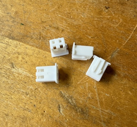
I have also standardized (somewhat) on JST-XH connectors and hook-up wiring for building nascent prototypes. Skiff designs at an early stage of development leads to frustrating and hard-to-fix shortcomings, like pots needing to be turned counter-clockwise to increase volume. Nice to be able to rewire things!

The initial build went fast, fast, fast

I laid out the jacks-n-pots board in less than 45 minutes:


From here it was smooth sailing--like building a kit. I already had a DUAL SOIC VCA ready to go--read more about the Irwin dual VCA here.


Since the dual concentric pots mount at 90 degrees they needed their own PCB.


initial tests....


WFT?


So did it work first time (WFT)?  Yes, but it soon kroaked (BISK).

After taking an evening off--which counterintuitively sped up troubleshooting, I came back to discover the problem was easily diagnosed: some of the 24 gauge wires I had soldered between boards were broken. As I tried to fix them, more broke, then fixing those, more broke. 

Arrg!

To ameliorate I came up with a simple bodge--using 100 mil edge connectors and shrink tubing on one side of each wire:


..............which ended up looking like this:


It would have been more elegant to crimp JST-XH 100 mil connects to both sides of the jumper cables but at this early prototyping stage this workaround was good enough.

WHAT NEXT?

The 3 PCB's specifically for the project--jacks board, front panel, and concentric pots board--could be improved in terms of layout; also I had a few ideas for making modulation bias adjustment--needed in some cases for a nice smooth stereo pan at audio out--easier to tweak. 

So....I will create revisions of the 3 PCB's, rebuild this in the coming weeks, and, if there is love, post it all on PCBWAY's community site. 

I already have the "version 2" boards laid out. 

I figure they will WFT? We will see. Stay tuned! 

UPDATE 4-10-25: Yeh, the improvements are done, and it all works!  See the PCBWAY community site page here--up and running.


AI generated background--hours of fun!


 OK enough for now--see ya next time.


Crimping JST-XH connectors--a Quick How-To

 It's a beautiful Spring day, instead of going out and enjoying it, I am teaching myself how to crimp and create JST-XH connectors. I b...