Readers: If you want to build the project featured in today's post, please go to PCBWAY's Community pages--a gerber ready to download and/or fabricate as well as KiCAD files, PDFs, a BOM, etc., are here.
Also please visit PCBWAY's site using the link here--it will help this blog immensely. Thanks.
For upcoming projects I needed a breakout board to turn any waveform in the audio frequency or low frequency range into a pulse wave. Then: use the output's rising edges and throw an interrupt on an MCU.
So, I needed a comparator; lots of ways to design and lay this one out, easy.
I also needed a few more features....
What I came up with:


DESIGN
As usual I recycled ideas used in previous projects.The MCP6002, an opamp I discovered looking at buffer subcircuits from Mutable Instruments, provided clamping. An easy way to clamp J6's ground to positive voltage was to limit the MCP6002's power pin, Vcc, pin 8, to 3.3 or 5 volts--whatever voltage my MCU expected.
The MCP6002's output will match Vcc--easy.
Warning: for any circuit that uses an MCP600x, do not supply greater than 6VDC to its Vcc pin--exceeding 6v may damage the MCP6002. If you need to use a larger voltage (say +12VDC for VCC) consider using a different op amp--pretty much any dual op amp will work, but you might lose the MCP6002's nifty clamping characteristics.
The MCP6002's second stage provided an inverted output, while J7's non-inverting output voltage was determinded by the voltage present at Vdd and not constrained to the clamp voltage.
VCC-VDD jmp wirepads could be shorted with a small jumper. This allowed the Vcc and Vdd to be supplied by a single voltage source.
The diode in U1A's feedback loop made U1A a precision rectifier, the same idea was used in a VCO triangle to ramp converter.
A final "feature": I could change output shapes with one additional part: C4. C4 can be omitted, but its value along with R2 provided a simple active filter, allowing different output shapes at J6 and different pulse widths at J7.
With R2 at 1K, values for C4 could be anything from say .01uF to 4.7uF and beyond. Omit C4 to get decently fast rising and falling edges at J6 and J7.
BUILD
 |
| New boards from the blog's sponsor, PCBWAY. |
 | |
|
 |
 |
| Whole board took minutes to populate--this was an easy one. |
100mil spacing for breakout boards presented a challenge to me, so I laid out J1-J7 200mils apart, grabbed some inexpensive 100mil edge connector material, and pulled out every other wire with needle nose pliers.
Now I have a 7 pin edge connector with pins 200mil apart. This made the board a lot easier wire up I thought and worked a lot better than anticipated.
 |
| power tested: no problems |
 |
| tested...worked! |
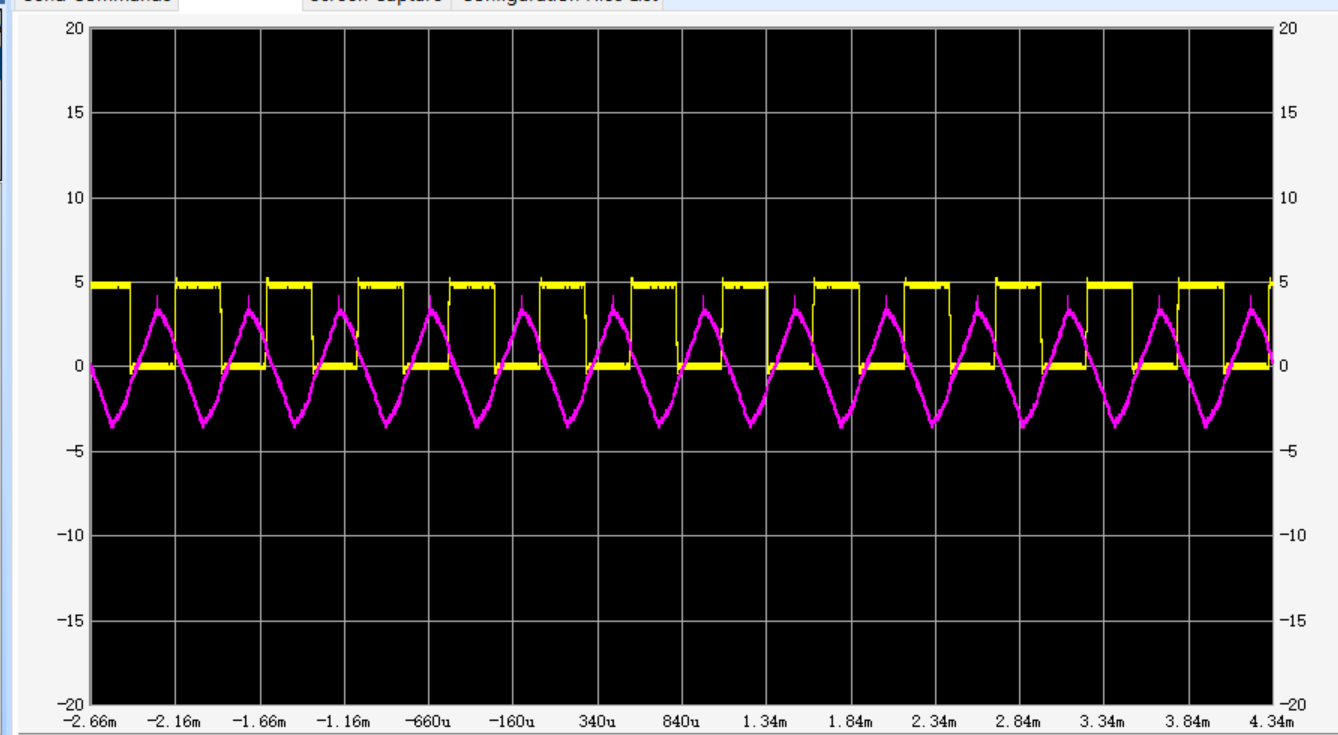
OUTPUT--WORKED!
Simple circuit, simple results. Purple trace is input, Yellow trace is output; screens were captured with Siglent's easy to use. This was what I was after.


So--I made a few errors with my silks but otherwise worked first time! When was the last time I saw that?
Onward!


No comments:
Post a Comment