Continuing a previous post, here's a simple buffer/clamp circuit to make sure analog to digital converter (ADC) pins in your Arduino or other MCU don't blow up due to excessive over- or under-voltage.
The design is simple: an op amp mixer with a zener diode clamp at its output. I have added a few other features as well.
Elements of this design will show up in future projects, but if you want to build this into a module for your rig or bench, get wiring diagrams, gerbers, schematics, etc., on my github here; you can also have boards fabbed at my sponsor PCBWAY's Project Pages, here.
Without further ado:
 |
| Instead of testing the revised/fixed buffer-clamp PCB working, then resigning it to purgatory in my "Prototype Fu" junk box, I created a simple frac module. Now I can use the clamp board on my bench and restrict audio or CV test signals to 0-5V by flipping the "5V clammp" switch. |
The board in the previous post here had some mistakes; here is the corrected, working schematic:

The result is a straightforward through-hole PCB that can be modified to suit most input/ADC buffering needs:

The board/module can be easily modified:
- For ADC's that max out at 3.3V, change the zener diode (D1) appropriately.
- The maximum offset voltage is normalled into the non inverting input of ICB3. It's determined by R2 and R10. It's set now to max out at 5V DC, assuming you are using a +/- 15V supply but different DC values are possible by changing out these resistors.
- I intentionally fed the offset voltage into IC3B pin 5; simpler would have been to introduce it in series with a 100K resistor to IC3A pin 2. I did this because in some projects I need to invert and offset a signal at input. I would place the incoming signal in series with IC3A Pin 1; R3 could be removed and the input signal presented there.
- The output impedance is set by R8 and R9. These values can be adjusted and for most applications are not critical; R9 could in some cases be replaced with a jumper.
- R12 and R11 set the range of the offset presented to IC3B Pin 5. Larger resistors here will create a more narrow offset range.
- Make sure the voltage dividers use reasonably high value resistors (>10K), so as to not strain your power supply.
- Hint: test your buffer before hooking it up to an MCU!
About the bench buffer: Let's add it to my bench setup.
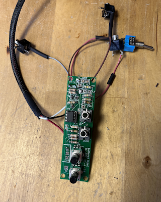
Some useless build photos:
 |
| PCBs sent fresh from this blog's sponsor PCBWAY. The shameless plug: Please help out this humble blogger and check them out.... |


 |
| Created front panel art with Illustrator |
 |
| Testing the bench tool on the bench! |
 |
| Front panel uses PCB material and "Mr Label" vinyl, see the posts here and here. |
 |
| Junk box parts! yeh! |
 |
| Testing the fit.... |
 |
| "Seems working!" |


