Monday, March 30, 2020

Smoke on the Forty--3340 that is--Actually a TL074--Burned up Sir!

Before any of this Covid/Corona Shelter in Place thing I could still invite friends to my studio. So I was showing off my CEM VCOs when all of a sudden SMOKE started pouring out of one of them.

Good work Elmo--nice craftsmanship--impressive job on this.

The OCD in me hates electrical smoke but I guess it gets us all at some point.

Here's the VCO PCB that blew up real good:

 I-IV-V: "wuz a TL074SMD.....now charcoal...."

Question: what happened?  The fried VCO was a CEM3340 based "prototype"--but then everything us DIYers build is a prototype right--anyway, the smoked VCO was the first 3340 VCO I built based on the design here. It didn't work at first, de nada, so I added kludge buffer daughter boards, a floating octave selector circuit, and extra 22 gauge wiring fixes affixed with hot glue, and more, all to correct my own design and fab screw ups; see the the previous post here....a horror show.

The front panel wasn't much better....

The other two CEM VCOs I built (post here) fared better--I used a "rev 2" PCB, correcting the mistakes of rev 1. That means: no kludges--and no smoke (yet) from either of these two (yet).


Lucky I was in the studio when the first VCO smoked right? Otherwise this could have really gotten bad.

So the question is, what happened? 

Well being not 100% sure....I dug in a bit.

The TL074 IC used as a quad buffer in the VCO has built in short circuit protection, here is the schemo of a TL071 shamelessly lifted from TIs datasheet:


This means that any current going in or out of a TL07x hits a few resistors first. I didn't know these resistors were there at all, but even so.....as I see it, with +15/-15V power, you're going to be sinking a max of something like 75mA of current through this tiny resistor if you create a dead short to Edison ground. That's over one watt. Since this is an itty-bitty-IC-in-chip resistor, not the honking LotsaWatt  resistors you'd find in a tube amp, the resistor can't be take that much punishment in terms of dissipating heat before saying good night.

There are also resistors between the + and - rails I can see in the TL071 schematic as well. Same sort of thing--you get a smidge of protection from overdoing the current from + to - from the looks of things, but there has to be limits to how much current you can put through any of these resistors before blowing up the FETS, transistors, or something else.

I like experimenting with innocent components....so I put a sacrificial TL071 on my bench, created a dead short from its output to ground (through an ammeter) than started cranking up the current from my bench supply.  WARNING: do not try this at home!!! The op amp will heat up very fast, you could burn your house down. PLEASE ALWAYS BE CAREFUL!

Here is my test circuit if you can even call it a circuit? The downward arrow represents my Fluke DVM set to read and display current:
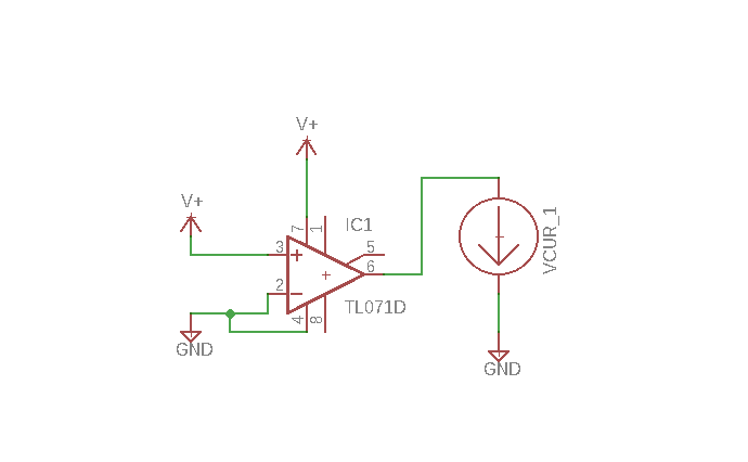
The op amp became hot very quickly when wired up like this.....and could easily have smoked if I left it a few more minutes, possibly taking other things with it, like my entire lab. Again PLEASE DO NOT TRY THIS AT HOME!

AudioDiWhy's lab dungeon of Op Amp Pain.


The data sheet says a max for the FK package (not sure what FK means, perhaps FK-U since this is TI? Help me out here?) is 260C for one minute. I didn't record exactly how hot the TL071 got in my experiments but within a few seconds it was too hot to touch. Probably way less than 260C.

So what happened inside the IC during the torture test? Not sure exactly. There might be clamping circuitry I don't see in the schematic....or maybe I am missing something, but when first powering up my torture test the ammeter read around 20mA, I figure because I wasn't reading true Edison ground, so about what I'd expect as the max source output current from the IC, for a few seconds. But then the Fluke read 0A and the chip started to heat up fast. Even at 5V V+ and GND, in the config you see above, once the IC clamped, things heated up, to the point where I couldn't touch the IC, after maybe 15-20 seconds. Not good.

So I think it's safe to assume that in spite of the short protection the TL07x IC will get really hot if you present the output with a dead short to ground. The heat has to go somewhere.....

I didn't bother testing things like reverse voltage present at V+ vs. V-, since I know that will kill the IC straight away (been there, done that). So: don't do that either.

So I figure, what could have killed the vco was simple: one of the outputs of the VCO's TL074 buffer must have gotten shorted to ground by a wire or kludge or solder bit or something. From the burn marks it might have been a short on pin 8 pulling way too much current through V-.


All Hail Richie Blackmore!


So what is my takeaway from all of this?

First--for modular applications, always use series output resistors for your output buffer op amps--at least 1K, on a TL0xx even though there is already a resistor inside. It isn't going to hurt to increase your short circuit protection.

Second--don't over kludge! This module was a horror show of daughter boards, hot glue, and 22 gauge bungies. Something was bound to go wrong, even though at first it "worked". Resist the urge--toss the overly kludged module and start over.

Third--Turn that sh*t off! YEP! always shut off all your DIY stuff when you are out of the studio, it's not UL listed and can blow up any time.


"Home, Charles": I took the smoked VCO out of the rack; time to rebuild it eh? I had left over extra rev 2 CEM VCO PCBs for this project--it was a pretty easy single evening job of using my rework tool to remove any parts I wanted to save from the blown out board and building up another main PCB, mounting it to remaining VCO guts, and calibrating it. Worked pretty much first time.

I also made the existing front panel a bit more presentable using "Mr Label", a vinyl sticker front panel process you can read about here.

Overall, good to have the 3rd VCO back, but I hope there isn't some sort of flaw in my VCO layout.  I guess we will see; if I indeed screwwed it up I will be breathing many more fumes at some later date.

Such is life sheltered in place.

Tuesday, March 24, 2020

Noise! Part III: Quad 4051 CMOS Mux

If you're like me, sheltering in place is a geek's dream, you can work at the bench all day and no one will bug you, since you might sneeze on them?

OK, I have been using this strange time to further expand and enhance the Noise! Lunetta circuit (read part I--basic board layout here; part II--digital quad pot control of 4x LunettaVCOs here).

This time I'm extending the Lunetta design from the creative mind of Martijn Verhallen/reverselandfill.org to respond to a 8x4 arduino controlled Mux.  This adds more audio oddness on 2x more output jacks.

The extra board allows CMOS "patching"--which Martijn's original design accomplishes with a jack bay--using CV control of an Arduino Pro Mini and 4x CMOS 4051 MUX SMD IC's.

Turns out, as with most things in Arduinoland, it was really easy to MUX this way.....I see this as a useful thing for any number of CMOS audio projects and I don't why I wasted so much time trying to do this with more complexity. 4051s are easy.

Here is the finished mux board (in front) buttoned up (???) on the bench.


CMOS fun and 4051 for audio is nothing new to this blog--see the voltage controlled switch synth  module here for instance. Yes the 405x chips are endlessly useful to what we do. BTW it wouldn't be hard to redo this board to use +12/-5 power and +5 logic, which should allow seamless switching of +/- 5V P/P audio signals--I have not messed with 405x powered this way, but it should work? The board would need to be modified to accommodate more voltage regulators, but really that shouldn't be too hard right? Maybe one of these days......


Prototype PCB for the Mux. $2 for 5x from China. Why stripboard or wirewrap, ever?


Once all the various pieces of the Noise! Lunetta are done (really, one of these days!) I'll post 'em on my website....

LOONETTA: The mux output goes to 2 output jacks--again thanks to Martijn's creative work--one an OR of each of 2x 4051s in the mux, the other, each 2 more 4051's outputs are fed through a series of 4070 CMOS XOR logic stages for some Korg inspired ringmod craziness.

The Mux CV is supplied right now by a 0-5V tall trimmer set up as a voltage divider, but I will add jacks and buffers for true CV of mux control in the next few weeks--for that I need yet another PCB. The post on "board # whatever" for the NOISE! project is coming up. Sorry I just can't stop!

OK, What does it sound like? --it sounds STRANGE.

I plan to do more sound clips one of these days, but take a look at this quick vid....it starts with a Turing circuit sort of situation, then inexplicably morphs into some audio farting, then back to Turing. This pattern continues forever. odd. More sound clips to come.....but not today, I am too busy working on the next PCBs for this project....


OK, on to the obligatory and possibly useless bench photos:


Here's the sketch that makes the whole thing go.  I can see many ways to improve this but for now hey it works:

  int CV0 = 0;
  int CV1 = 0;
  int CV2 = 0;
  int CV3 = 0;

  int MAP0 = 0;
  int MAP1 = 0;
  int MAP2 = 0;
  int MAP3 = 0;

void setup() {
  pinMode(1,OUTPUT);
  pinMode(2,OUTPUT);
  pinMode(3,OUTPUT);
  pinMode(4,OUTPUT);
  pinMode(5,OUTPUT);
  pinMode(6,OUTPUT);
  pinMode(7,OUTPUT);
  pinMode(8,OUTPUT);
  pinMode(9,OUTPUT);
  pinMode(10,OUTPUT);
  pinMode(11,OUTPUT);
  pinMode(12,OUTPUT);
  pinMode(13,OUTPUT);
  pinMode(14,OUTPUT);
  pinMode(15,OUTPUT);
  pinMode(16,OUTPUT);
  pinMode(17,OUTPUT);
  pinMode(A0,INPUT); //tie to mux pins D2-D4
  pinMode(A1,INPUT);  //tie to mux pins D5-7
  pinMode(A6,INPUT); //tie to mux pins D8-10
  pinMode(A7,INPUT); //tie to mux pins D11-13


}

void loop() {

 digitalWrite(17,LOW); //enable IC5
 digitalWrite(16,LOW); //enable IC3

 CV0 = analogRead(A0);
MAP0 = map(CV0,0,1023,0,7);

 CV1 = analogRead(A1);
MAP1 = map(CV1,0,1023,0,7);

 CV2 = analogRead(A6);
MAP2 = map(CV2,0,1023,0,7);

 CV3 = analogRead(A7);
MAP3 = map(CV3,0,1023,0,7);

////////////////////////////////////
//IC2

switch(MAP0)
{
case(0):
digitalWrite(2,LOW);
digitalWrite(3,LOW);
digitalWrite(4,LOW);
break;

case(1):
digitalWrite(2,HIGH);
digitalWrite(3,LOW);
digitalWrite(4,LOW);
break;

case(2):
digitalWrite(2,LOW);
digitalWrite(3,HIGH);
digitalWrite(4,LOW);
break;

case(3):
digitalWrite(2,HIGH);
digitalWrite(3,HIGH);
digitalWrite(4,LOW);
break;

case(4):
digitalWrite(2,LOW);
digitalWrite(3,LOW);
digitalWrite(4,HIGH);
break;

case(5):
digitalWrite(2,HIGH);
digitalWrite(3,LOW);
digitalWrite(4,HIGH);
break;

case(6):
digitalWrite(2,LOW);
digitalWrite(3,HIGH);
digitalWrite(4,HIGH);
break;

case(7):
digitalWrite(2,HIGH);
digitalWrite(3,HIGH);
digitalWrite(4,HIGH);
break;

}

/////////////////////////
// IC3
switch(MAP1)
{
case(0):
digitalWrite(5,LOW);
digitalWrite(6,LOW);
digitalWrite(7,LOW);
break;

case(1):
digitalWrite(5,HIGH);
digitalWrite(6,LOW);
digitalWrite(7,LOW);
break;

case(2):
digitalWrite(5,LOW);
digitalWrite(6,HIGH);
digitalWrite(7,LOW);
break;

case(3):
digitalWrite(5,HIGH);
digitalWrite(6,HIGH);
digitalWrite(7,LOW);
break;

case(4):
digitalWrite(5,LOW);
digitalWrite(6,LOW);
digitalWrite(7,HIGH);
break;

case(5):
digitalWrite(5,HIGH);
digitalWrite(6,LOW);
digitalWrite(7,HIGH);
break;

case(6):
digitalWrite(5,LOW);
digitalWrite(6,HIGH);
digitalWrite(7,HIGH);
break;

case(7):
digitalWrite(5,HIGH);
digitalWrite(6,HIGH);
digitalWrite(7,HIGH);
break;

}

/////////////////////////
// IC4
switch(MAP2)
{
case(0):
digitalWrite(8,LOW);
digitalWrite(9,LOW);
digitalWrite(10,LOW);
break;

case(1):
digitalWrite(8,HIGH);
digitalWrite(9,LOW);
digitalWrite(10,LOW);
break;

case(2):
digitalWrite(8,LOW);
digitalWrite(9,HIGH);
digitalWrite(10,LOW);
break;

case(3):
digitalWrite(8,HIGH);
digitalWrite(9,HIGH);
digitalWrite(10,LOW);
break;

case(4):
digitalWrite(8,LOW);
digitalWrite(9,LOW);
digitalWrite(10,HIGH);
break;

case(5):
digitalWrite(8,HIGH);
digitalWrite(9,LOW);
digitalWrite(10,HIGH);
break;

case(6):
digitalWrite(8,LOW);
digitalWrite(9,HIGH);
digitalWrite(10,HIGH);
break;

case(7):
digitalWrite(8,HIGH);
digitalWrite(9,HIGH);
digitalWrite(10,HIGH);
break;
}


/////////////////////////
// IC5
switch(MAP3)
{
case(0):
digitalWrite(11,LOW);
digitalWrite(12,LOW);
digitalWrite(13,LOW);
break;

case(1):
digitalWrite(11,HIGH);
digitalWrite(12,LOW);
digitalWrite(13,LOW);
break;

case(2):
digitalWrite(11,LOW);
digitalWrite(12,HIGH);
digitalWrite(13,LOW);
break;

case(3):
digitalWrite(11,HIGH);
digitalWrite(12,HIGH);
digitalWrite(13,LOW);
break;

case(4):
digitalWrite(11,LOW);
digitalWrite(12,LOW);
digitalWrite(13,HIGH);
break;

case(5):
digitalWrite(11,HIGH);
digitalWrite(12,LOW);
digitalWrite(13,HIGH);
break;

case(6):
digitalWrite(11,LOW);
digitalWrite(12,HIGH);
digitalWrite(13,HIGH);
break;

case(7):
digitalWrite(11,HIGH);
digitalWrite(12,HIGH);
digitalWrite(13,HIGH);
break;
}


} //end loop

In CMOS we trust!! Yeh Elmo, turns out something simple like this works just fine.

Next up, I am going to add some VCAs to this; more tall trimmers for CV adjustomatic, I have a few other ideas for more add-ons.

One of these days the NOISE! synth will be done and racked up, but for now, it's just too much fun building more stuff for it; like the winchester mystery house will it ever end? Stay safe!

Saturday, March 7, 2020

Piece of PAIA: 2720 Bandpass VCF Lives Again!

Howdy again, it's time to get into the time machine and go back to 1974, let's build an audio filter in the spirit of the legendary synth kit maker, PAIA. To wit; a 2700 series filter, that was my first synthesizer, built it with my brother from a kit, and after many hours of fab it sounded pretty damn crappy as I recall.

But hey it got me started down this path right?

PAIA still has a place in my heart, so when I was cruising on the E-M DIY forum and found a reworked schematic of the classic PAIA 2720-3B Bandpass filter from gasboss775 so I said hmmm.....

The original PAIA design is the super low parts count you'd expect:


This was reworked by gasboss with different variations....to me, the one that looks like it catches the spirit of PAIA hegemony is this one:


Yeh the 2700's VCO's wouldn't stay in tune and its low pass filter was a trailer tragedy, but I remember the 2720 3B bandpass filter sounding a bit better than the rest, especially when buffering its output with the PAIA 2712  inverter buffer module.

Looks like some of the EM members strip-boarded the gasboss rework and it works!

But me--strip board?  Who needs that? Let's fab up a PCB and try it out:


Back from China and it took me about two hours to fab on my bench:


Tall Trimmers are used for this revision for convenience.  I'll probably change that out for rev 2.


Notice the incorrect name of this board on the silk.  It's a 2720, not a 4720.  And also how JLCPBC messed up my part # to better have theirs prominently displayed. But then again--what do you expect for $2 for 5 boards?

Ready To Test!


PAIA in the FACIA: At first my build of gasboss' 2720 variant sounded rel bad--all sorts of issues with driving the filter cutoff, tons of distortion at output, and other maladies.

After a couple of evenings of messing with the circuit and some malodorous swearing, I realized I forgot a critical resistor in my schematic capture: R12, which was screwing w/ the frequency cutoff.  Easily kludged in....

OK That fixed some of the CV issues but the VCF still sounded a bit, well, mild (but I remember the original 2720 VCFs not having a lot of drama either).

After more experimenting, I discovered that using a BOWAL front end (post about that is here and here) to precondition incoming CV helped the sound a lot--the filter seems to respond best when I have control of not just CV level but also CV bias, and then if I crank the CV way down into bipolar-CV-land the gasboss 2720-3B starts to sound a bit more juicy.

I have to think about why that is for a while, but whatever; I will do a revision that includes a BOWAL subcircuit/incoming CV buffer--the CV input should be buffered anyway....

The output needs to be buffered/boosted as well; I fully remember that being the case on the original 2720-3B.

OK: it's time to revise the layout and then do this all again. I'll do a follow up post and hopefully create some sound samples.

UPDATE: 6-9-20 Board is finished, I added a 2nd board and made this thing skiff.  2720 filter Post Part II is here. Website post about this project is here. Soundclip using finished 2720's is here

That's it for now--until next time, don't breathe the fumes.

A guy OK with C tries to learn C++. Bjane me Up, Stroustruppy!

Why no posts so far for 3-2024?  I have been woodshedding, brushing up on C++ skills.  What got me to finally start digging into C++? I was ...