Showing posts with label Kicad. Show all posts

KICAD 10: Hierarchical Sheets and Blocks: Lay 'Em Out Once, Use 'Em Again

Readers: today's post assumes you have a working knowledge of Kicad, an incredible open source EDA program. If not, this post might be pea soup. Newbies: watch a great Kicad tutorial here.  And--previous audioDiWHY posts focusing on Kicad are here, here, here and here. 


I have read that good engineering is modular engineering. Is good audio synthesis modular audio synthesis? 

Not sure.

Kicad--our beloved schematic capture/PCB layout/simulation software--has recently added some great features in making bits of your previous designs reusable--a huge timesaver.  

Let's go over this.

"Hierarchical Sheets"

....let you put subcircuits into other designs, treating the subcircuit as a "black box"--don't worry what's in the box, just enjoy what it can do....you expose I/O between your black box and main design using "hierarchical labels."
  • Because I'm lazy, I will abbreviate hierarchical sheets going forward as "HS"
  • Create a new project, this will contain your HS.
  • In the schematic (.sch file), put whatever components you want in your HS--you are creating a normal schematic at this point.
  • For I/O you need to share outside your HS issue the command: "Place" > "add hierarchical labels"


  • Save the schematic.
Next--Create a new parent project; in the next few steps, we are going to embed the "HS" content into it.
  • In the parent's .sch file, click on this icon on the right:

  • using this tool, draw a box inside the parent schematic. 
  • You will see a blue box...this represents the HS:


  • A properties dialog appears (if you don't see it, select the "Untitled_Sheet" and then tap the letter "e".)
  • Give the HS a name
  •  in "sheetfile" click on the folder icon and navigate to the kicad_sch file you created initially, the one that contains your HS.

  • At this point you might see dialogs about using relative filenames and something about database tables being messed up (?).  
  • Pretend you didn't see any of that and click OK twice.
  • Still in the parent schematic, click on this icon on the right:

  • Click on the HS box; the I/O pins ("hierarchical labels") created in the the source .sch file appear in the parent schematic--they are placed sequentially
  • Create the rest of the parent schematic and wire it to your HS.
In the screenshot below I ran a DC simulation on a parent schematic containing a hierarchical sheet; the HS contained a single 100k resistor with "in" and "out" labels. 

The simulated DC voltages in dark red show that this works--the 100K resistor in the HS is hidden from view but is part of the simualtion.
This is an OC simulation--DC values--not to be confused with "OCD"


DESIGN BLOCKS

....allow you to create a subcircuit, save it in its own library, and import it into future designs. 

This feature showed up in Kicad 9 (See the video here). 

With Kicad 10, you can put schematic symbols/wires and PCB traces into a single design block.

And--again, due to indolence/laziness, I will call "design blocks" going forward "blocks". Have a nice day.  

Organizing blocks: Blocks are organized into libraries, same idea as Kicad symbols.  Each block is a folder containing a json description file and file(s) for the .sch and/or .pcb components.  

For both the people out there who are interested--get a zip of my custom blocks from Github, here.

Creating a block: select some or all of your design, then right click on "blocks" 


From the drop down, choose "Save Selection as Design Block"


But! Be careful about "hide library tree", if you click that, the entire block's user interface section disappears. This threw me at first. I had to go back to view > panels > design blocks to make it reappear.  
 
Tidbit: By clicking "New Library" you can also choose if you want the block to be visible in the current project only or globally (all projects); the default is global:


Viewing existing Blocks: from the schematic editor View > panels > make sure "design blocks" is checked.... you see something like this (your block names will be different....)


Using existing blocks: Double left click on a block, drag it into your schematic, creating a group of components and wires.

Editing blocks:

  • Select either PCB 
  • Right clock inside the block and say Grouping > ungroup
  • Edit.

Before


After: now it's editable components like everything else in the schematic.


NOW: A WORD FROM THIS BLOG'S SPONSOR

OK, you just created something awesome using these new Kicad 10 tools and need to get some PCB's, then get them assembled.

For this, check out this blog's sponsor, PCBWAY, who can fabricate the PCB's, do the component assembly, and then, do everything else.

In addition to top shelf PCB fabrication they also do fantastic work with 3D printing, injection molding, and much more. 

And!!! Kicad Mavens (you must be if you've made it this far?): run, don't walk, and submit your Kicad masterpiece to PCBWAY'S Kicad PCB Design Contest--winners get cash and/or RPi goodies. Check out the contest here.

As always--you can help this blog by checking out the PCBWAY site.  Thank you!


SCHEMATICS AND FOOTPRINTS/TRACES IN ONE BLOCK--New to Kicad 10--How To Do This

Super useful--capture the schematic and layout of a subcircuit in a single block. However--work slowly and carefully. This feature is one of those "miss any step and the whole damn thing won't work" situation.  

The steps:

Creating the combo block--start with the schematic:
  • Create a schematic subcircuit with all the symbols, wires and values you want in your block.
  • Tool > create associations  
  • Make sure everything is OK, that all symbols have associated footprints and so on.
  • Create a block--for this let's call it europower w traces


Next, create the associated traces.
  • Go to PCB and update the PCB from footprint
  • The footprint appears
  • Draw in all traces you want to include in the combo block
  • Save the selected footprint and traces (you must select both!) as a block  (right click on block > save selection as block)
  • For the block name, type in the exact same name you used for the schematic block--this is case sensitive: in this case, "europower w traces"
  • Kicad 10 will ask "overwrite block"?  Say YES

To use it:
  • In your schematic, pick the block europower w traces and put it on the schematic
  • In your PCB, pick the same block europower w traces and put it on the pcb
  • Hit F8.  
  • If all goes well you will see a footprint with traces appear--the PCB and the schematic are "synced"--it's all wired up.
  • If you messed up, a new footprint will appear with no traces. Fiddlesticks! Try again, make sure to follow each step.
  • You can now grouping > ungroup your Schematic or PCB block and change things.  


Tidbit: I noticed when upgrading Kicad 9 > 10 I had to set the global blocks path manually.  Preferences > Manage Design Block libraries > global libraries:


For Kicad 10.0.1, I had to set the Nickname, the "Library Path" (where the global block libraries are stored--the local location might vary if you are using a cloud repo on different hosts), and the Library Format (pulldown to "Kicad") by hand for this to work. Not sure why this didn't come over with the rest of my preferences.  

OUTTRO

Think "She's so Heavy": another brilliant John Lennon time signature change, with rapid master tape cut.  

Canva Affinity and Kicad 9: Graphical Madness for DiWhy Projects

Many thanks Elton at Otter Mods for introducing me to Kicad and Affinity.

============

When I look at professionally created front panels, surrounding knobs I often see "goes to 11" gradients:

                             
(what are these called?  "Gradients"?  "Tick marks"?  For this post I will call them "dials"....)


Using the built-in graphics tools in Kicad 9 didn't get me far, but found I could import graphics into Kicad as footprints, then add them to PCB's used as front panels on a silkscreen layer. 

OK, how?

There are two graphics import methods in Kicad I know of:  

First--easy: through Kicad's "Project Manager"--a tool you see when you first open the program--I could turn PNG graphics into bitmaps, using the Image Converter tool. 


Works, but, I found at times the output was grainy.  

Update 5-25-26: to motorize the Image Converter tool in Kicad 10 I vibe coded a uv + python based PNG to SVG converter, get it from github here--create Kicad-ready SVG's files, using PNG graphics as yur source, drag the SVG into a Kicad PCB, pick your layer (usually front or back silk) and scale it. 

So far, works surprisingly well.

What else?

Elton at Otter Mods, the resident Kicad expert of my geeky tech group, described a better way:

Use Affinity Designer to create SVG formatted files, then import the files into Kicad as footprints. Finally, place the graphic footprints on your front panels.

Today's post outlines a workflow to do this--this may be documented somewhere, but I couldn't find it, and ChatGPT was out to lunch.

CANVA AFFINITY 

First I needed to get Canva Affinity, Elton's choice for creating SVG graphics. 

Tough choice. Pay enormous bucks for an Adobe Creative Cloud subscription, complete with hidden fees, a confusing cloud presence, and terrible tech support? 

Nope. Good news: like Kicad 9, Canva Affinity is free. 


Or is it? I had to set up a Canva account, last I heard the friendly Canva folks aren't a 501C, rather someone has to buy lunchroom donuts and most important: keep the shareholders happy.  

Whatever....I set up a "free" Canva account, downloaded Affinity, and installed it on my W11 PC. 

So far, so good.

After a few hours of trying out the new Affinity: it felt like a true Adobe killer, combining features found in Illustrator, Photoshop, and InDesign, into one mega-graphics app. Affinity can do most everything Adobe can do, it seems.

For creating dials I focused on Affinity's VECTOR persona which closely matched features found in illustrator.  

It had an Export > SVG feature--so far, so good.

CREATING THE DIAL

Knowing squat about Affinity vector I watched this video which contained a lot of what I wanted to do. 

An aside: I found a lot of online documentation for Canva Affinity out of date; perhaps Affinity, like Microsoft, has no problem changing their UI early and often, like soiled chonies;  Internet documentation (and AI) is slower to catch up.  

....they moved around the furniture?
.
After an hour or so I ended up with this:


A few notes; I won't remember any of this 2 days from now.

  • I chose a 120mm x 120mm artboard and made sure the outer circle had a 100mm diameter. How to set up artboards and canvases in Affinity is covered in this video--video is not for the UI current as of 12-1-25 but I could follow it. The 100mm diameter made the size conversions described below easier to figure out.

  • I used grids/guides. Good video for that (again, for an earlier version of Affinity Designer but the steps still seem current?) is here. However, there does not appear top be a way to save a custom grid configuration, unfortunate. Here are the settings used:


  • To make the tick marks, use Affinity's Vector "power repeat" feature; take a look at this  how-to video. I had to make sure to set the checkboxes and adjust rotate points as described in the video or I'd end up with an ugly mess. 
  • The repeat settings used for the big ticks:


  • I then created a smaller tick over the large one at 12 o'clock, dragged its rotation point to center (red line and green guide lines visible) and repeated with rotation of 7.5 and number of copies of 64. 

Couldn't find anywhere: how I created the gap between 7PM and 5PM at the bottom of the dial. 

By trial and error, here's how; most everything I found online appeared to be uselessly out of date: 
  • Use the Affinity Vector knife tool
  • If you zoom way in on the circle the knife tool becomes the scissor tool—yeh, I knew that.
  • Make the start and end cuts on the arcs, where we need to get rid of parts of the circle, by left clicking with the scissor tool
  • From the main menu: vector > separate curves 
  • Using the move tool (not node tool!) click between 5 and 7; 
  • The arc to be deleted is boxed with a faint blue rectangle.
  • Hit delete on your keyboard
  • Arc that was boxed is now gone
  • Use node tool to further clean up any ugliness.
Finally I exported the 100mm x 100mm dial using File > Export > Export > SVG > SVG (for export).

AND NOW--A WORD ABOUT THIS BLOG'S SPONSOR


As soon as you have your front panel design and gerber you will need your work fabricated. For this, you should use PCBWAY.

PCBWAY, the sponsor of this blog, has a service to fabricate PCBs and other materials using any color of the rainbow. That's full color PCB's folks! Details are here. I will be covering this super cool service in a future post.

In addition to top notch PCB fabrication they also do fantastic work with assembly, 3D printing, injection molding, and so much more. Their staff is super friendly and PCBWAY always turns the work around quickly. I am always impressed!

You can help this blog by checking out the PCBWAY site.  Thanks.

IMPORTING INTO KICAD


In Kicad 9 I used the footprint editor to create a new footprint library then a new footprint for the dial.  SVG's import: file > import > graphics.

.....this dialog:


This seemed straightforward until I discovered the "Import Scale" was linear but inaccurate. 

Meaning, if I set Import scale to .5 and imported a 100mm circle the resulting footprint was not a 50mm circle. 

Damn!

Not sure if this is documented anywhere--probably is, but, I couldn't find it--I ended up crafting this formula which seemed to get the job done:

X = Z/(A*3.08)

Where:

  • X is the # to use for Kicad's import scale
  • Z is final size you want
  • A is the original size of SVG
Why 3.08?  No idea, I figured it might be PI, which got me close, but no, 3.08 yielded better results.  

For instance, for a 100mm diameter, and 25 mm output, I used this.

X = 25/(100*3.08)

X = .0811

BINGO.


For 100mm source, and 15mm target:

X = 15/(100 * 3.08) 

so x = .0487 to use for import scale, here’s what I got in Kicad. BUTTER!


I found that for smaller inputs (e.g., 50mm circle SVG instead of 100mm) the outputs drifted a bit, not sure why, but was still good enough. In general, I figured: why not stick with 100mm SVG source files. That's what I did here.

Summarizing--here are some common Input scale: values to use based on a 100mm SVG source. Target footprint size in millimeters is the column on the left.

8 0.025974026
9 0.029220779
10 0.032467532
11 0.035714286
12 0.038961039
13 0.042207792
14 0.045454545
15 0.048701299
16 0.051948052
17 0.055194805
18 0.058441558
19 0.061688312
20 0.064935065
21 0.068181818
22 0.071428571
23 0.074675325
24 0.077922078
25 0.081168831
26 0.084415584
27 0.087662338
28 0.090909091
29 0.094155844
30 0.097402597
31 0.100649351
32 0.103896104
33 0.107142857
34 0.11038961
35 0.113636364
36 0.116883117
37 0.12012987
38 0.123376623
39 0.126623377
40 0.12987013


Before wrapping up--one more thing. Affinity allowed me to jump between "Vector" ("Illustrator") and "Pixel" ("Photoshop") mode. Great, it meant that I had more cool editing tools at my disposal. But--I found that SVG's modified in Pixel mode often created a file that Kicad couldn't import. I found it best to do all the work in the Vector Persona.

WHAT'S NEXT?


This whole SVG > Kicad thing can be used for more than dials. Line art?  Yep. Logos? Sure. Any single color or BW 2D graphic import that can be turned into a line drawing should work. 

I uploaded my footprints from this SVG > Kicad silk workflow into Github (here) and will try to keep the repo current.

For the full color materials, Affinity would be a great way to get into that. I'll cover this in a future post....

And of course I will add more dials and graphics to future projects using the methods above.  

Overall, many enjoyable hours down the rabbit hole for this one. More to come.


Kicad, NGSPICE and the MiniMoog EG Simulation Rabbit Hole

This one started when my 50-year old (!) Minimoog bit the big one.

Its Loudness Contour Envelope Generator croaked; it would work on occasion if I tapped on the DECAY TIME knob--so, a faulty potentiometer?

I took it to an expensive vintage electronics repair shop 45+ minutes away. 

Sadly, $600USD later, after "fixing" it, the sustain knobs sent CV to the VCA and VCF, even if a key wasn't depressed. Need to do a soundcheck? Have the roadie crank up "Sustain Level". Done.

Not a feature, a bug?

MiniMoog "Modifiers" section. On my vintage Mini this is transistor/resistor/cap/diode only ADSD Envelope Generator.

In the words of Richard Nixon: I had to erase it myself?  

If so, I needed to understand how the Mini's EG worked.

Looking at MiniMoog schematics (here and here), its EG's are discrete; no IC's. 

I had (and still have) almost no experience with circuit design from this era: pre-integrated circuit, but post-vacuum tubes. 

The more I tried to study the schematics and follow signal paths the more my brain hurt.  

I tried to simulate the MiniMoog's Loudness EG using Falstad:

Get a functional (pun intended) MiniMoog Loudness Contour simulation here. I couldn't get this Falstad simulation to work, but Mod Wiggler's "guest"--the same superhero who helped save the triangle to ramp design in the DVCO project, here--fixed my broken Moog EG sim. Yeh!


Cool...I had a working simulation, but try as I might, I could not duplicate the odd "Sustain to CV" fault on my beloved MiniMoog.

So--I did what any rational person would do--I gave up. 

Of course, I couldn't leave it alone. 

Instead, I went down a design using only discrete rabbit hole. 

Nevertheless, I dug further into Falstad to (try to) whip up discrete simulations for LFO's, preamps, and EG's. 

I quickly learned that, like my brain, the UI for Falstad wasn't up to some of it.

Which led me to--sorry about the long intro, folks--the NGSPICE simulation abilities built into our beloved EDA software--KICAD 8.  Simulating discrete component circuits for me was way easier than endless breadboarding.


TUTORIALS 


To simulate circuits, Kicad (an open source project) incorporates code from another open source project, NGSPICE; NGSPICE'S beginner's tutorial page is here but the how-to doesn't help much for Kicad.   

To learn Kicad 8's NGSPICE user interface: watch at least some of the 7-part video series starting here. This is essential viewing.  The content creator presents his tutorials slowly; he's thorough, easy to follow, and accurate--worth the time.  

GETTING STARTED--FAKE DC POWER


Something that puzzled me--how could I "turn on" a simulation?" There is no breadboard to wire anything to, no PCB to fry with a bench supply.

To provide fake power to a fake circuit: in a Kicad 8 schematic, I placed a component called SPICE > VDC:

Spice VDC component


I added the usual +5V power pin and GND to this VDC spice supply.  

I edited its properties, renamed it V1, and gave it a 5 volt DC voltage; when my simulation power was ready to go it looked like this:

 Once +5VDC was defined somewhere in my schematic, I found I couldn't define a Spice VDC for +5V again or cryptic errors would appear when it came time to simulate the circuit.


 To create a phony bipolar supply I could craft something like this:

                                                         Simulated +/- 15V Power supply 

With this in place, I could use +5, +15, GND and so on, "powering up" my circuit during simulation. 

Moving on:


555 ASTABLE: FIRST SIMULATION

Back when dinosaurs roamed the earth I built an astable using the venerable 555 IC.  As an homage, for my first simulation using Kicad, I started there.

555-the newbie's IC!


But! Putting a 555 symbol, passive components, and my +5VDC power supply into a Kicad schematic, then starting the simulation (steps to start a simulation follow shortly), threw cryptic errors.  

Turned out: the simulation didn't know what to do with a 555 IC, since its behavior needed to be defined or "modeled". 

I found models for just about every common component I could think of using Google searches--often they are found on manufactures' websites. I gathered a few model files I thought I'd use frequently and put them on Github--here. 

Here's a quick summary of how to add a model to a Kicad symbol:

  • Select the 555 symbol in the schematic
  • Tap "e" key to select properties
  • Click on the "Simulation Model" button:


  • Point the component to the 555 simulation file and choose the 555 model:
If the path to the file might change on other computers you work on, consider using a Kicad variable like ${sim_model} instead of hard coding D:\[path to this] [path to that]


Click on the PIN assignments tab to make sure the pins from the model map to the pins in the Kicad symbol:


With this in place--was I good to go?

The best thing about simulations--you won't blow anything up, ever. Go ahead: try weasel, try squirrel!

I started the simulation using Inspect > Simulator

I created a new simulation using the "plus" icon:


I chose: "OP - DC Operating Point". OP was akin to using a voltmeter, so I figured--easy?


....and to my surprise it showed voltages and current for a sim as a snapshot in time: IT WORKED!!!  

Cool!!!!!


SCOPE A DOPE


Seeing voltages and currents at a point in time was great, but I wanted to take it up a notch: see an X as time and Y as amplitude. 

I put the 555 astable schematic into a hierarchical sheet (a brief how-to covering Kicad hierarchical sheets is here--go to the bottom of the post).  

Using this 555 astable to generate a couple of pulses in 30 seconds I crafted a three transistor attack/release envelope generator:


To edit an existing simulation, I used this icon:

TRAN--something the GOP will outlaw before long? No, blogs like this go first. 


I chose, as my type of simulation, "TRANS", an abbreviation for "Transient Analysis", the simulation akin to capturing the output of an oscilloscope. 

"Time step" formed the sample rate, "final time" constituted how many seconds of data my fake scope's Y axis showed:


I found that making time steps too big or too small could bring the simulation to its knees. For this simple A/R function generator, plotting every 10ms and doing so for 30 seconds did the trick.

With the simulation successfully launched: to choose the voltage I wanted to see plotted over time, on the right column I chose "V(OUT)", indicating the label I added to the AR schematic seen above.


I ran it and it worked! The V(OUT) looked pretty good--attack and release resistance impacted the circuit's peak output voltage but for 3 transistors: good enough.

I also needed to get a 2N7000 simulation model for this as well. I found it here--again, a manufacturer's website is a good place to start your model file journey.


DIGITAL SIMULATION


With my pseudo-analog AR design working I was on a roll--could Kicad be used for digital simulations? 

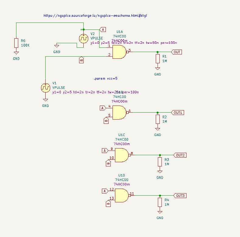
Specifically: some older ADSR's have SR latches (the "discrete ADSR" here for instance), could I get an 74LS00 simulation to work?

Once again the tutorials here and here  made this pretty easy; I got the models for some of the 74HCxx IC family here--downloaded from the link next to "models for 74xx digital devices, a NGspice subset derived from the MicroCap library."

Setting up the simulation was not too difficult, but I found I couldn't skip a step and have it work--these tips are in the aforementioned videos, but, here they are again:

  • I tied outputs I wanted to see in my simulation to an 1M resistor, which is in turn tied to GND. Otherwise, the simulation wouldn't work.


  • I made sure I added this text to the simulation's .kicad_sch design (this assumed "5V = high" logic):

I have no idea why this is needed....just do it.


  • I didn't need to worry about the power pins on a simulated digital IC, at least for the 74xx series mentioned in the video.

  • Since I was doing a transient analysis of a digital simulation, I unchecked "Save all Currents" and "Save all power dissipations" and selected "PSpice and LTSpice" as my "compatibility mode" (you knew this, right?). Otherwise the simulations throws cryptic error and warning messages and may not run.


With all of that--and it all had to be right for any of it to work--I got a 7400 simulation going:


Notice that no power section "E" is needed.


Output.


OTA's


I simulated those too....took me a day to figure out I needed to use the VSIN (voltage) spice part, not the ISIN (current) part. Doh! That simple mistake tripped me up for hours. 

Again, you can get the model files I have tested working with Kicad/NGSPICE here.

13700...Could only find a model for 1/2 the IC.  The "1/2 LM13700" symbol is available as in the library file found here.

CA3080


Seems worked: green is input sine, output is amplified signal (I got the 13700's built-in Darlington buffer to work, and also an op amp based buffer)


PLOTTING FREQUENCY RESPONSE


To wrap it up I drew a simple schematic, in this case an RC filter:


I used a 2 pin connector for the input, not a spice component.  

Clicked on J1, clicked E for properties then chose the Simulation Model button:


 Under settings--I selected "built in SPICE model"'; Device Type: DC and AC magnitude Value 1; DC value 0:


For the simulation I set up "AC small signal analysis" with these values (stop frequency for audio should be anywhere from perhaps 10Hz to 100K)


When I simulated the filter I got a nice roll off plot:


Good for trying what-if's, dropping in different cap and resistor values--seeing what happens--why do math, ever?

Good video that goes over AC Small Signal Analysis in Kicad 8 is here.

THIS BLOG'S SPONSOR!


Before I go, got to shout it out for this blog's sponsor, PCBWAY. Once you have your simulation working, it's not hard to turn it into a real .sch/.pcb and gerber file and send it off to PCBWAY.  They will get it back to you super fast....PCBWAY fabricates at incredibly low prices (5x 2 layer boards for about $5 US.....).  Hats off to them, I am grateful for their sponsorship of this blog.

ABRUPT TAPE SPLICE 


That's it for this time, paraphrasing the great Quintus Arrius: "you have the spirit to watch bad YouTube, but the good sense to control it". Simulate well and live! See ya next time.