Showing posts with label VCO. Show all posts

AD9833 Audio VCO--Works But not Finished


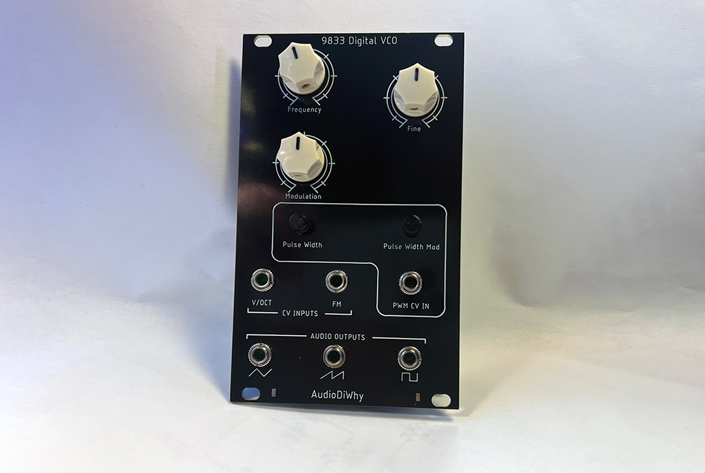
 I finally have the AD9833-VCO working! Eurorack format.

The fun starts with the AD9833 post here. I wrote a C library for it....then I did this thing with the AD9833, then this thing, then that thing, then something else--I have to link all those posts?

Too lazy, if you want to know the history of the function generator IC used in this VCO, please search this blog for "VCO". 

This blog is chock-a-block full of posts about the handy AD9833--I have written more about this function generator IC than I should have....to cut my teeth on embedded C, SPI, UARTs, and everything else we know and sing. 


WORKS, BUT NOT FINISHED!

This has been a laborious project--as always, still, more work needed....

The 12-bit Seeed ADC buffer board--good for a lot of projects--may not be the right solution here. Best I can tell, 12 bit data gets lost in the A-D noise floor (I think?) and thus the audio output of the VCO is a bit jittery. I want to fix that. I could use a 14 bit ADC and just toss out the 2 LSB's. That might help?

Also the triangle to ramp PCB's ramp output (previous post here) a bit too buzzy sounding. There are ideas on Muff Wiggler about ameliorating that puppy.

For now it works, the VCO doesn't smoke, looks OK, tracks V/octave fine, and damn, I need to get this Rube Goldberg thing off my bench for a bit!

THE SIGNAL FLOW:


I mostly designed and built this VCO to see if I could figure out how to design and build this VCO. Makes sense?  There are lots of designs out there for audio synthesizer VCOs that are a lot simpler. This isn't one of those.

How it works:

Input is a volt/octave CV, modulation CV, and a frequency and fine control.  

These are mixed, buffered and clamped by the buffer board that incorporates a SEEED XAIO RP2040 dev board (see the previous post here, the buffer PCB is a PCBWAY community project; PCBWAY sponsors this blog--thanks!--if you want to build one, you can get the gerber here).  

The RP2040 on the SEEED dev board is running embedded C (current code revision of the code is on Github, here).  

It uses a python frequency lookup table array creator--which I turned turned into a .h file for this project (github repo for the Python array frequency creator is here). 

I also used the AD9833 C library I wrote for AD9833 (github here) and debugged using UART (post here). SPI is used to drive an AD9833 (again, lots of posts about this IC, for the VCO I used this cheap breakout board).  

The AD9833 has a 600mV unipolar triangle output--so yet another PCB is used to convert the triangle to ramp and pulse/PWM and buffer the 3 signal outputs....post for this subcircuit is here, modwiggler forum thread about the concept and design of the converter begins here

Yes, this is a complex build!  To make it even harder, the build uses no hookup wire and is configured in Eurorack skiff format. That makes it difficult to modify and inconvenient to troubleshoot, but, well, who likes things to be easy.

Build Photos:

Board fab was from this blog's sponsor, PCBWAY--please help out this blog and check 'em out.


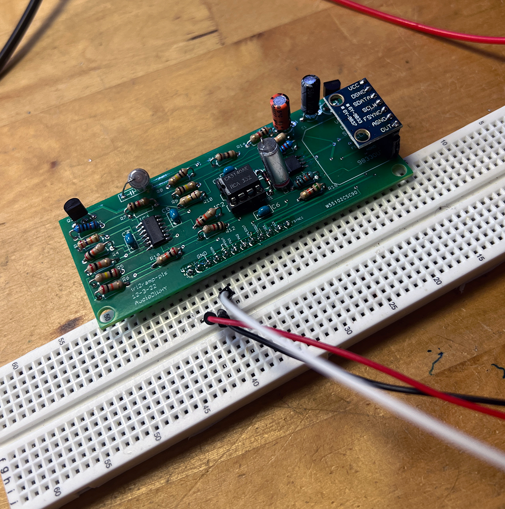
testing the triangle to ramp converter....it works....


OUTTRO


I blew up a SEEED dev board getting this going, one AD9833 BoB was defective, and one SEEED board was DOA. A lot of swearing and head scratching has gone into this project so far.  Doh!

This experience has been pure DiWHY--such as, why am I building such a complex VCO when a 3340 based analog equivalent will probably sound better and be a hell of a lot easier to lay out and build?

DiWHY masochists: show you can take the pain and get yer zips for BOMs, gerbers, PDFs for the schematics and boards, and Eagle CAD files for this VCO, at Github here

If anyone wants to join in with further madness, message me through the MW forum and you can play along. or just grab the files and start modifying.  

In the meantime I am going to take some time off DiWhy--my pychiatrist fiance (amazing she accepted my marriage proposal right?) tells me I need a break. The Good Dr. is always right.

work on other projects for a few weeks or more to regain my DiWHY sanity. 

Then go back to this project. 

For instance, I already have a 14 bit ADC board to replace the 12 bit version used for this project. To skiff-ize the PCB, it uses a lot of tiny tiny SMD parts...should be a real pain in the butt to fabricate. Blah blah ginger blah blah? update 3-5-23: turns out the 12 bit ADC was fine, or at least good enough, issue was with other elements of the design.

....this project tied a lot of previous learning into one module, and getting it to perform better (better sounding ramp, better ADC performance, other improvements) will be good learning as well. I will say it yet again: in the words of immortal Emil Faber: "Knowledge is good"
 
Update 3-5-23: newer version of this VCO is here--greatly improving the design I think.

Back to work.

RP2040-AD9833 VCO--Triangle to Ramp Waveform Conversion

Hello again! This time I continue design and fabrication of a Eurorack audio VCO based on an RP2040 dev board and AD9833 function generator

the bench battle begins.....

I discussed the volt per octave ADC and MCU in the previous post here.  The V/octave PCB worked on the bench, but the AD9833's output leaves a bit to be desired for DIYaudio:

  • Its output is 0V to 600mV--we need more bipolar beef!
  • It can output triangle, sine, and square, but only one waveform at a time.

How can we turn this puny triangle signal into the bipolar 10V peak to peak triangle/ramp/pulse found in a traditional analog VCO?  

A common way achieve triangle to ramp conversion is to invert the "downward slope" of the triangle.  The inversion means instead of the waveform going up and down it only goes up.  

Easy right?

You can use an op amp to invert things:


...but as per my lab notes you have to turn on and off the switch at exactly (and I mean, exactly) the right time!


How can we create this critical switching signal?  

That's the tricky part! I had some (complicated) ideas using comparators to trap the top and bottom of the triangle, or maybe an ADC and MCU, but my notions seemed overly complex. 

There must be a simple way to do this, but how?  

At the advice of a friend I turned MODWIGGLER DIY FORUM for help.

MW is an amazing resource!  

After posting my problem some really talented techs jumped in with suggestions; the thread on MW is here

Guest from OpenMusicLabs conjured up a simple Falstad Simulation--fantastic!

Guest's from OpenMusicLab's design--you can see the sim he created here.


I drew up a schematic based on his idea--my schemo also provides for a pulse width modulated square wave, which I fully stole from the DIY legend Thomas Henry, as well as a buffered triangle output:

Values changed for the bench prototype (so far): C3 and C6 are are .0022uF; zener is 5V; R18 is 50K.

I turned that into a PCB to try out on the bench.....

Then I sent the gerber to this blog's patient and always helpful sponsor, PCBWAY, who quickly got it back to me:

My usual shout out to the folks at PCBWAY, please help out this geekly blog and give them a look for your next round of fab....

Cool! 

Did the PCB work right away?  

Nope.  

It wasn't a mistake in the design, nor in the converter circuit's basic concept, rather, I suck at breadboarding and was sloppy with soldering....I don't know exactly what it was, but all the wires and parts and alligator clips and things all my bench over drove me nuts.  

After blowing up a SEEED RP2040 **and** a 9833 breakout board, cleaning up bad solder joints, trying out some different cap values, and wasting a lot of time due to stupid breadboarding mistakes, yes, I got it to work.

The horror....

The horror....

The ramp wave created wasn't perfect but it was pretty close; it sounded a bit gritty, which was A-OK by me.  The distortion at zero crossing was less evident at lower frequencies where it counts most.  


Distortion at 4k; it diminished at lower frequencies


There was further discussion on ModWiggler about how to clean up this distortion. For instance, don't use a 2N7000 MOSFET for the switch, use a comparator. Update 2-27-23--putting a .01uF cap between pin 1 of the 2N7000 and ground improved this switching distortion somewhat. I will include this mod in a future "improving the tri to ramp converter" post.

The conversion conversation continues....this is an extremely helpful and enthusiastic community, and I am grateful for all the techs who helped with this design to date. 

OK I will put the AD9833/RP2040 and this waveform conversion board into a single package to make a Euro module VCO prototype in the next post. I will also make it easy to swap in different waveform conversion boards so the design can be further refined by making the VCO truly modular, from a design and layout perspective.

If I have time? Really folks, it's time to keep moving forward. Please stay tuned.

Smoke on the Forty--3340 that is--Actually a TL074--Burned up Sir!

Before any of this Covid/Corona Shelter in Place thing I could still invite friends to my studio. So I was showing off my CEM VCOs when all of a sudden SMOKE started pouring out of one of them.

Good work Elmo--nice craftsmanship--impressive job on this.

The OCD in me hates electrical smoke but I guess it gets us all at some point.

Here's the VCO PCB that blew up real good:

 I-IV-V: "wuz a TL074SMD.....now charcoal...."

Question: what happened?  The fried VCO was a CEM3340 based "prototype"--but then everything us DIYers build is a prototype right--anyway, the smoked VCO was the first 3340 VCO I built based on the design here. It didn't work at first, de nada, so I added kludge buffer daughter boards, a floating octave selector circuit, and extra 22 gauge wiring fixes affixed with hot glue, and more, all to correct my own design and fab screw ups; see the the previous post here....a horror show.

The front panel wasn't much better....

The other two CEM VCOs I built (post here) fared better--I used a "rev 2" PCB, correcting the mistakes of rev 1. That means: no kludges--and no smoke (yet) from either of these two (yet).


Lucky I was in the studio when the first VCO smoked right? Otherwise this could have really gotten bad.

So the question is, what happened? 

Well being not 100% sure....I dug in a bit.

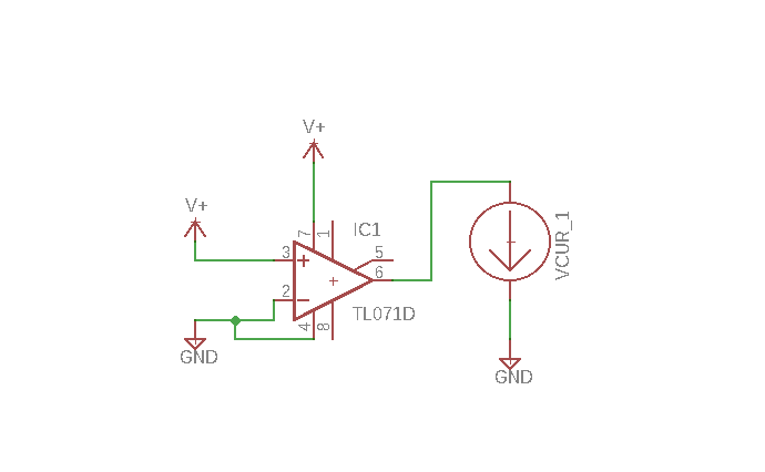
The TL074 IC used as a quad buffer in the VCO has built in short circuit protection, here is the schemo of a TL071 shamelessly lifted from TIs datasheet:


This means that any current going in or out of a TL07x hits a few resistors first. I didn't know these resistors were there at all, but even so.....as I see it, with +15/-15V power, you're going to be sinking a max of something like 75mA of current through this tiny resistor if you create a dead short to Edison ground. That's over one watt. Since this is an itty-bitty-IC-in-chip resistor, not the honking LotsaWatt  resistors you'd find in a tube amp, the resistor can't be take that much punishment in terms of dissipating heat before saying good night.

There are also resistors between the + and - rails I can see in the TL071 schematic as well. Same sort of thing--you get a smidge of protection from overdoing the current from + to - from the looks of things, but there has to be limits to how much current you can put through any of these resistors before blowing up the FETS, transistors, or something else.

I like experimenting with innocent components....so I put a sacrificial TL071 on my bench, created a dead short from its output to ground (through an ammeter) than started cranking up the current from my bench supply.  WARNING: do not try this at home!!! The op amp will heat up very fast, you could burn your house down. PLEASE ALWAYS BE CAREFUL!

Here is my test circuit if you can even call it a circuit? The downward arrow represents my Fluke DVM set to read and display current:
The op amp became hot very quickly when wired up like this.....and could easily have smoked if I left it a few more minutes, possibly taking other things with it, like my entire lab. Again PLEASE DO NOT TRY THIS AT HOME!

AudioDiWhy's lab dungeon of Op Amp Pain.


The data sheet says a max for the FK package (not sure what FK means, perhaps FK-U since this is TI? Help me out here?) is 260C for one minute. I didn't record exactly how hot the TL071 got in my experiments but within a few seconds it was too hot to touch. Probably way less than 260C.

So what happened inside the IC during the torture test? Not sure exactly. There might be clamping circuitry I don't see in the schematic....or maybe I am missing something, but when first powering up my torture test the ammeter read around 20mA, I figure because I wasn't reading true Edison ground, so about what I'd expect as the max source output current from the IC, for a few seconds. But then the Fluke read 0A and the chip started to heat up fast. Even at 5V V+ and GND, in the config you see above, once the IC clamped, things heated up, to the point where I couldn't touch the IC, after maybe 15-20 seconds. Not good.

So I think it's safe to assume that in spite of the short protection the TL07x IC will get really hot if you present the output with a dead short to ground. The heat has to go somewhere.....

I didn't bother testing things like reverse voltage present at V+ vs. V-, since I know that will kill the IC straight away (been there, done that). So: don't do that either.

So I figure, what could have killed the vco was simple: one of the outputs of the VCO's TL074 buffer must have gotten shorted to ground by a wire or kludge or solder bit or something. From the burn marks it might have been a short on pin 8 pulling way too much current through V-.


All Hail Richie Blackmore!


So what is my takeaway from all of this?

First--for modular applications, always use series output resistors for your output buffer op amps--at least 1K, on a TL0xx even though there is already a resistor inside. It isn't going to hurt to increase your short circuit protection.

Second--don't over kludge! This module was a horror show of daughter boards, hot glue, and 22 gauge bungies. Something was bound to go wrong, even though at first it "worked". Resist the urge--toss the overly kludged module and start over.

Third--Turn that sh*t off! YEP! always shut off all your DIY stuff when you are out of the studio, it's not UL listed and can blow up any time.


"Home, Charles": I took the smoked VCO out of the rack; time to rebuild it eh? I had left over extra rev 2 CEM VCO PCBs for this project--it was a pretty easy single evening job of using my rework tool to remove any parts I wanted to save from the blown out board and building up another main PCB, mounting it to remaining VCO guts, and calibrating it. Worked pretty much first time.

I also made the existing front panel a bit more presentable using "Mr Label", a vinyl sticker front panel process you can read about here.

Overall, good to have the 3rd VCO back, but I hope there isn't some sort of flaw in my VCO layout.  I guess we will see; if I indeed screwwed it up I will be breathing many more fumes at some later date.

Such is life sheltered in place.

3340 VCOs: Finished!

Happy day! The 3340 VCOs, based on TH's Maximus design, are good to go. Got some expensive panels back from FPE, along with PCBs that fixed the DOH! mistakes in Part IINASA: we have 2x VCO modules with DIY PCBs, DIY panels, and DIY mods, that work great.


To review:
  • Part I, where I create an V/octave switch using TI's REF02 IC, is here.
  • Part II: where I stuff the first set of VCO PCBs to come from China, and fix the dumb mistakes, is here.
  • Part III--love at last--wait, that's this post! it all works!  
The obligatory and probably fully unnecessary bench photos follow.

...no 3340 yet.  I always test the boards for shorts before putting on the expensive ICs. Another tidbit: I had to use 25 turn trimmers for scaling, expensive but worth it--we want our VCOs to really be V/oct right?

Yeh Baby!  Yeh!!!!

Of note: about the REF 1V/octave switcher board. Yep, for these 2 VCOs I "improved" it (not a bug--a feature?)

Read more about the basic octave switcher for this here; to sum up, I could have used hand-matched 1% resistors, a rotary switch, and an op amp, like most everyone else, but wanted to try new things, and also hopefully get better performance in hot and cold environments. To that end, the PCB uses a REF02 chip from TI as a 5V reference. Next, high performance .1% SMD resistor arrays that stay put, value wise, in inclement weather are used to as voltage dividers.

Each stage of the V divider is wired to a switch; I ended up having to spring for pretty good switches....finally to an OP07 op amp used as a unity gain buffer.

So far so good?

There is a problem with my design first described in PART I, towards the bottom of the post, again part I of this post is  here.

To reiterate: TI's somewhat vague datasheet has an example where they suggest using a trimmer (not shown or really explained in their docs? But why, Brian, why? Come on TI, help out an old dumb rock and roller!) to set the exact output value of the reference chip relative to ground (pdf here--see page 7). To save money and PCB space, and to avoid the fear and loathing caused by having to figure out vague TI circuit examples, I skipped all that.

But: omitting this overall 5V ref trim was done at my peril?

No, happy ending!

Here's the issue: After wiring up the board: choosing GND (0V) as a voltage setting on the front panel V/oct. switch was a few mV off vs. REF02's 5V output. This makes sense--GND knows nothing about whatever the REF02 IC is producing at its output. And I have no way to trim the REF to be exactly 5V relative to Ground (I left that off, remember?)

And of course I can't change GND feeding the V/octave switching sub-circuit without some really stupid extra work.

That meant that when choosing the 0V octave setting, the VCO would suddenly go out of tune vs. the other VCOs in my rack.

OK what to do about our butt switch setting?

I didn't want to go back to square one for the v/oct board design. Instead, let's mod: I cut the GND trace on the octave switch board and used a 24 gauge kludge wire (brown wire seen in the photo above) to connect the GND rotary switch setting to the tip of a 3.5 inch jack. Ha! Take that! Now you have LFO, 2', 4', 8', 16' (I think 4 octave switching is good enough) and this new jack: "EXT". Into this external input you can blast FM mod, audio, CV, whatever, then choose your goofy mod signal, any time you want, with the octave switch. This turned out to be a fun addition to the VCOs user interface, and if I had thought through the ref board design with a bit more care it would have never happened.

Lesson learned: it pays not to think too much?

Note the whacked font for "LFO" and "OCTAVE SELECT"...I was so ocd'd out with getting the drills just right that I missed this illustrator flub! CRAP! I want my panels to be perfect; but a fellow synth club dude says I'm being hysterical....


The whole process of building all of this was a lot of work but enjoyable....

I have parts to build about 2 more of these VCOs....not sure I will right away, too many other things to do....


Good to have stable VCOs but perhaps too much time and money? You can get 3340 kits already good to go, EG: here and here.....you might want to go this route instead of what I did? Me, I'll take door number er....I mean door # two.

At some point I'll post the finished PCBs for this VCO on my website; the 3340 board schematic is not my design so i don't feel good about posting it, but Scott Sites and TH are cool so it's posted here.

I left out the suboctave and sine wave stuff but otherwise the PCB is a total match.

Time to move on; already working on the first DIY synth full kit I've touched in like 12 years. The kit thing so far has been a struggle, and my psychiatrist girlfriend questions whether it's time for me to not solder for at least a week. Too many fumes?  Can't say--ask the good doctor.

Until next time: have fun, then enjoy the post-Curtis glow.  See ya!

CEM VCO Part II: Maximus Troubleshooting, and the DOH! Count

From a couple of posts ago: My ASMVCO's are getting old and drifting in pitch.  Might be time to ditch 'em. how about three new VCO's based on the repop of the Curtis 3340 VCO chip?

Module ready to test ("MRT's").  If the module works OK for a couple of weeks I'll create a FPE  front panel for and retire the kludge panel.


OK got rev one of the three boards back from China, got it stuffed and put behind a temp panel. It works!  Holds tune for at least 7 octaves, I have trouble hearing the really high stuff no matter what but let's assume that works as well.


Ho-MORE DOH-KIE: I am using 3 interconnected PCBs to minimize hook up wire: a main board (3340 chip, buffers), an octave switcher (see previous post here--btw, the  TI REF02 based add-one-volt-per-rotary-click seems to work great so far, guess I got lucky?), and a PCB to hold the "Thonk" type PCB 3.5" jacks. The Thonks connect to the main PCB with a 10 conductor IDC ribbon. The octave selector was supposed to mount to the front panel, but I melted my cheapo switches, so for this rev 1 build I used a clunky junk box NOS rotary switch wired to the board, post for the octave board madness is here.

OK, the main board is based on  "VCO Maximus", another classic from the mighty Thomas Henry. A good page on the Maximus for Eurorack is here.

I chose this 3340 design vs. all the other ones out there because a guy I know in my synth meetup group already built a couple of these on strip board; he told me Maximus works and sounds great. I omitted things like the sub octave circuitry and sine wave conversion from triangle; I already know how to do that and have plenty of sine waves and sub oscs in my modular setup now, so these 3x VCO's will just be pulse, saw, and triangle. Good enough.

Old trick: print out the PCB 1:1, lay it over the panel, tape it, punch it and drill.  The drills will line up.

So how did rev one of this module do? Considering the complexity of the board, happy to say: not too bad; I got the basic VCO to work in about a day. I had to kludge things, I made several mistakes that needed fixing for this revision, see below, but so far everything but the sync in, which may be broken or just sounds crappy, is on the air. Update: sync is fixed.  I had the DPDT switch wired wrong. The VCO stays in tune, the waveforms look good on a scope, PWM, linear and FM mod all work. Happy day.

Also the pots turn the right way (clockwise for more of whatever), that's good. I was worried about that.

A
"Obligatory Bench photo"

I modified a left over alubase 2u Frac panel I had lying around so as to not have to test this module with circuit guts flopping everywhere. The drills on the junk panel didn't line up with the PCB's for this project; that's what Dremel tools and drill presses are for.

Almost ready to test?

OK it works, but, let me go over the mistakes. I document this (and everything else in my blog) mostly for me--if I write this down I might not keep making the same mistakes!!

And for levity (?), instead of only bitching I am going to rate my mistakes with Homer Simpson DOHs. Let's begin:

First mistake: Four DOHs! the ramp wave output was busted, I just got a 15V DC at Output, no saw wave, no audio.

Using my scope I could see the saw out worked before the buffer, but not after.

But why, Scotty, why? I traced everything out--no mistakes. I pulled the SMD chip with a HAR and replaced it, same issue. Turns out I did a butt dumb thing: I had an op amp stage flipped, so what should have gone into inverting went into non-inverting. I missed this while translating the Maxiums schematic from the web to Eagle. I have been making this flub since I started laying out PCBs and I am a bit surprised I missed this when proofreading my work--well, I did. To sum this up:

 The moral: Always check Op amp + and - inputs. "I only give negative feedback!" Get em backwards on stripboard, PCB, whatever, and the damn thing will never work.

I fixed this by lifting parts, soldering components together above the PCB, and using hook up wire to put things back where they needed to go. After a day on my bench all of that broke (resistors detached from traces, solder connections shorting together, it was horrible) so I ended up creating yet another small daughterboard for the ramp buffer. So much for cutting down on hook up wire? not pretty, but it works.

Second mistake TWO DOHS:  I used the "net names" feature in Eagle to connect a pulse pin connector to the jack trace, but I called the trace "PULSE" on one side and "8" on the other. Naming nets/traces in Eagle CAD can make your layouts easier to follow but you have to get it 100% right. When you incorrectly join nets, Eagle won't tell you you made a mistake--it will dutifully connect things as instructed, but your board won't work the way you want.

Oddly I have never made this net names mistake before now, but Gabba gabba hey! This was fixed by cutting a trace and using a single 22 gauge kludge wire. Now I have a working pulse at output.  Oh yeh, see how pin 10 is unused?  Why didn't I put the ground on that? Instead I had to run a hookup wire for ground. I add that into the 2 dohs calculated. I will fix it next time.


No, Elmo, these 2 traces won't connect!

Third mistake: ONE DOH  
I forgot to connect ground to one of the pins of the rotary switch PCB.  I will let myself off the hook on that, I was kludging stuff here to accommodate the NOS switch replacement for the bang good crapola rotary switches, and I just missed this.  I also forgot to put a ground run into the 10 conductor ribbon. Wait, I already said that. Both easily fixed in rev 2. Yes there will be a rev2.


Fourth mistake: SIX DOHS!  OK this one gets 6 out of five. I left the entire buffer for pulse out of the REV1 PCB design. I have no idea what I was thinking. Did I think it didn't need a buffer? Overall I  wasn't looking at the Maximus schematic carefully enough I guess. I fixed this by digging into my junk box of tiny buffer PCB's and added the circuit fragment you see below as a daughter board to the main PCB. Since this was buffering a square wave I used a junk box CA3140, which may not have made any difference at all.


OK I think that's it. Last night I plugged in the new VCO and yep--it all works. I may not make a lot of design mods for rev2, rather just incorpoerate all the fixes, but who knows.

UPDATE: I had more PCBs made correcting these mistakes, new ones don't need kludges!  Yeh! post is here.

UPDATE 11-23-19 After a few weeks of having this VCO in my rack the top end v/oct scaling was still not quite where I wanted it to be (it was close, but was still a bit off when I went say 5 octaves above middle C).  After a fair amount of messing with the trimmers to set low and HF scaling, I replaced the 12 turn trimpots with Bourns QV36's, which are 25 turn.  They cost $3USB each from Digikey but it's worth it. Now with the more precise timmers the VCO scales much better, so I am going to add that to the BOM--25 turn pots.

UPDATE: All well and good, but this initial VCO ended up smoking and almost burning down my house. Too many kludges! Glad I was there to cut its power. Otherwsie I'd be writing this update from the public library's public PCs. Post about smoking this VCO is here.  

Stay tuned.

CEM VCO Part I: REF02 Based Octave Switcher

I've been using three DIY ASM VCO's for over 12 years now, and they work fine, but they drift a bit in hot weather, the PWM on one breaks, and they collectively use 9U of Frac, a lot of space.

Time to get some new VCO's going to complement the 13700 VCOs I built a while back....

How about basing them on reissued 3340 Voltage Controlled Oscillator ICs?


You may have heard 3340's before, they make VCO builds easy and fun: the tough parts--temperature stability, PWM, synch, 1V/octave response, etc., are all sorted within one IC. 

These ICs along with other Curtis offerings were popular in the late 70's to early 90's, in the Prophets and OB-X's and whatnot. Then they became harder to find for years; now with the resurging popularity of modular audio synthesis they have been cloned and/or reissued and are back with a vengeance.

Let's get building! 

Let's not start with designing an octave switcher. The MiniMoog has that; the SH5 has that, the MS20 has that..... 

On the SH5 this feature is called "Range". the rotary switch lets you quickly choose octaves: clunk chunk chunk--I like it!

That means somehow producing 0V, 1V, 2V, 3V etc, accurately, and presenting this stepped voltage as a modulation source to the 3340 VCOs.

But how, Scotty, how?
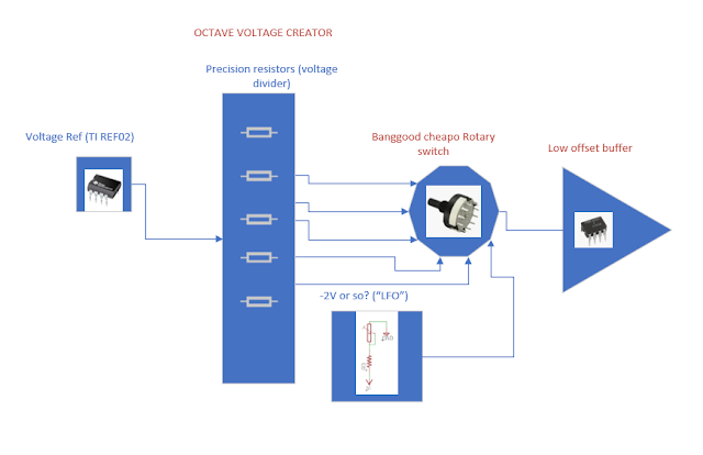
I studied schems for Minimoog and a few others, and based on that, here is the idea:


OK, the reference voltage IC, in this case TI's REF02 5V, feeds a voltage divider consisting of 10K .1% resistors that stay stable in spite of  hot and cold, an octave select rotary switch, and finally a buffer for the output voltage, which means a decent performing op amp configured for unity gain. 

In this case for the buffer I will use a TI OP07--mainly because I got a bunch of OP07 SMT's at a good price from Tayda.


Breadboard Time: I had a REF02 DIP in my parts box as well, no idea where it came from but it's been there a long time. OK, let's put that chip into the unflappable Radioshack learning lab with some 10K 1% resistors. 

It seems to work!  I can safely assume the rotary switch won't add any resistance and wiring up an OP07 as unity gain buffer is simple, so I didn't bother bread boarding those.  

Whipped up a schematic in Eagle:


....and came up with this board design:


I want to keep each VCO to 2u Frac so I decided to use SMD for as much as I can for this board. I did this to save space and make to things more challenging.  

OK sent that off to China for fab, and it's back:


( I know--IC2 is backwards...fixed in the photo below)

What you see:

  • The Yellow box out is the REF02. 
  • The red shows the location of the voltage dividers, I used an incredibly tiny 4x 10K .1% 10ppm resistor array  from Vishay (ACASA1002S1002P1AT) and a 10K .1% SMT resistors.  
  • The Blue box shows the location of the OP07 op amp.


Here it is in a vice ready to test:


....and that's where the problems began:

  • The rotary knob selected the wrong voltages, at least partly because the Eagle footprint I used matched the geometry of the banggood rotary switch, but not the way the switch is wired up electrically. So what should have been pin 3 on the switch was really pin 1, 2 is 2, 3 was 1, 4 was 12, and so on. A mess! I checked three times to make sure the switch would fit physically, but assumed the pin out would match. "When you assume"....OK I needed to fix that and redo the PCB design.
  • I burned up a few REF02s and one OP07 because there is a mistake in the silk screen. From the photo above: on the bottom left where you see GND: The V- and V+ are silk screened backwards.  DOH! Easily fixed, I wired it opposite the silkscreen, still....dumb mistake.
  • I burned up another REF02 because I shorted out its input supply voltages, this was due to sloppy wiring from my bench power supply. That one was avoidable!
  • OK with all that fixed, here was the bad news: The output voltages were just WRONG
  • Wrong, wrong, wrong!!!
To address these issues I used a Sparkfun hot air rework station to extract the SMD parts one by one. I lifted some traces under one of the REF02's by overheating, thus ruining the entire PCB, but at least the parts could be reused.

After a lumbgurius amount of cursing, fear and loathing I discovered the problem has something to do with the rotary switch itself. 

When I removed it from the PCB I could put a DVM on each step of the voltage divider ladder and my DVM would read 5V, 4V, 3V etc, to about 3/500th of a volt, which for me was probably adequate. 

But why the switch (or the buffer? the traces? something else?) was introducing crazy errors in output voltage is a mystery to me. I had to redo the board anyway to accommodate the banggood switch pinouts but still....I wasn't sure if fixing that would fix the voltage issue. 

I confirmed that the rotary switch was at least part issue; after removing it from the board and spinning it I would get unreliable continuity from its inputs to its output. 

Wiring it up back up to the board with pin out errors fixed didn't help things at all. I felt that it was extremely easy to overheat the switch's contacts, which might have happened when soldering the part to the PCB. I am pretty sure I melted the switch's guts with what I thought to be normal soldering. Oops....


I also noticed that the unity gain buffer daughter board was having its own reliability issues, so I swapped the OP07 for an SMT TL071. 

To my bemusement I found the TL071, purchased from Tayda, didn't have any designation re: where PIN1 was (no dot, no line--nothing) which may account for the bargain basement price of USD35c each. I figured I had a 50% chance of getting it right so I flipped a coin and dropped it in with the mgr. logo facing where pin1 should be? UPDATE: Not Tayda's fault, **my fault for not researching this carefully enough**. the Tayda chip has, upon close examination, a sloped side and a flat side. The sloped side "points to pin 1" on SMD chips. Read about how to find PIN1 for SMDs on the webpage here.

OK now presenting 1 to 3V DC into the unity gain buffer board's input, the tiny op amp PCB worked flawlessly.

But still: Employing the rotary switch the circuit's output remained spotty--it worked occasionally but most often was unreliable.

Not one to give up....I got an old 6 position switcher from my junk box:


After throwing in this ancient rotary switch the circuit worked perfectly. No hiccups, no dropouts, no issues. 


Test time: I soldered a 3.5mm jack on the unity gain board and a set screwed a chicken head knob on the repaired REF02 circuit's NOS switch, and tested it using a Mutable Links to accurately sum the output of my octave generator and the output from a Kenton Midi to CV converter.  Plugging this into a couple of 1V/octave VCO's the octave tweaker prototype worked well enough, I felt, to proceed with redesigning the PCB for a more reliable rotary switch. I had to bump a VCO's fine tune slightly after changing to a new octave every now and then, but I have to do that now on my beloved 1978 Minimoog and ancient Roland SH5 as well--so: good enough.

Bang-Good-Riddance: It's time to put the cheapo Banggood rotary switches into the e-waste recycle bin. Once again I spent all day trying to fix a problem with a poorly made component and maybe I saved $10 on the "affordable" component vs. something more reliable.  Not a good decision.  I am finding good hardware is worth the extra money.

And I also have an entire VCO to build. Stay tuned.

UPDATE: I got new boards made for the REF2 based octave switcher design. For this I planned on using prepurchased, relatively expensive switches: NKK MRK206's. There is an eagle symbol for it, that's one of the main reasons I used this switch vs. all the other ones you can get from say Digikey.

Got the boards, got the switches, guess what! The expensive switch DOESN'T FIT!  Turns out the NKK MRF206 symbol fits the MRK206 switch and visa versa.  I think whoever was creating the NKK library for Eagle got the 2 parts mixed up. 

Go figure--the lesson learned again: never trust an Eagle symbol! Print out the PCB before fab, lay the parts on top, and make sure everything lines up.  Oh well...toss the boards and try again.....

Pins don't line up!


UPDATE 12-8-19: PCB has been redone (again) to fix the pin issue above. For the new board everything lined up and worked. But--a design flaw I hadn't considered--1V, 2V, 3V all all within 3/500mV to each other, but GND is one of the selections as well, and it's not privy to the relative tuning coherence for the rest of the output V's.  So 1V is 0.95666, 2V is 1.95623, 3V is 2.95362, etc., which is fine, since there is a "master tune" tweak on the main VCO board, but also, GND is -6mV!!  I am thus concerned that the "2 foot" setting will be out of tune with the other octave settings. I can't see why it won't be, but I guess we'll see.

Finished Octave switchers, with NKK fancy 6 position switches.  


UPDATE 1-5-20: not a bug a feature! I cut the trace allowing me to choose ground as one of the "V/octave" settings and wired a jack to it. See the update immediately above--GND is not in lockstep with the switched voltages so using it as a switch setting was not feasible. But 2' or whatever isn't a useful setting anyway. Now, with this EXT switch in play, we have LFO, "external", 2', 4', 8', and 16'.   

UPDATE 1-22-20: VCO is done and the ref board (with the mod above) works! More info in the finished VCO post, here.  Part II of the VCO build, where I troubleshoot stupid mistakes on the main PCB, is here.

UPDATE 3-22-23: Hope this is the last update?  I just realized a dumb mistake I have been making for my VCOs incorporating the switch in this post: in the pipe organ world, 2' is the highest frequency, not 32' which is the lowest!  So, the panels I made have this silkscreen on incorrectly. Doh!