Arduino Againino....R4, ATTINY and UPDI

 After years of staying away from the Arduino--too many abstractions getting in the way of knowing how things really worked--I was drawn back by the Uno R4 Minima.


UNO ARRRR 4 MINNIMEE, MATE!  

Shiver me Timbres! 

Feature-wise, the R4 looked a bit like the cool and popular Teensy. It features a 32-bit Renesas RA4M1 ARM Cortex M4 processor, 14-bit ADC's and a built-in 12-bit DAC. 

It's a performance improvement from the Uno R3's 8-bit processor and 10-bit ADC's. 

I bought two R4 Minimas and updated my Arduino IDE to the current version. 

I also purchased a few R4 workalikes from SEEED: the XIAO-RA4M1:

Seeed XIAO RA4M1 is a truly dinky Uno Minima R4--the connector seen here is USB-C, giving you an idea of its small size.


The R4 can be easily programmed from the Arduino IDE; for me, plug it in and go. 

After making sure a blink sketch worked, the next thing I tried was the analogWave.h library. 

The library let me whip up audio frequency waveforms fast, fast, FAST, with only a few lines of code:  

////////////////////

#include "analogWave.h" // Include the library for analog waveform //generation

analogWave wave(DAC);   // Create an instance of the analogWave //class, using the DAC pin

int freq = 10;  // in hertz, change accordingly

void setup() {


int pin = 0;

 analogWriteResolution(12);

 wave.saw(freq);

 //limit of freq seems to be about 30hz to 10k for this library


}

void loop() {

  // Read an analog value from pin A5 and map it to a frequency range

  freq = map(analogRead(A5), 0, 1024, 0, 10000);

  wave.freq(freq); 

}

//////////////////////


When I connected the R4's DAC to my scope I was pretty disappointed--the output looked "stair-step": 


I found TriodeGirl's sketch that produced a better sounding ramp wave from the same hardware--but  relied on banging the stuffing out of the MCU's registers; if I was going to do that, I might as well stick with the RP2040 and 2350, which I felt were better documented.  

TriodeGirl's Audio output--looks much better--saw @ about 366hz.


OK, how about creating an audio frequency sawtooth waveform using analogWrite()?  

I wrote a single value to the DAC, and on the next run through loop(),increased the output amplitude by one; when the output amplitude got to 255, returned it to zero.

That didn't work perfectly either; the output looked "hairy":


Read more about this error here.  

I decided I'd pass on the R4's DAC for all but the most "DC" applications. 

Beyond that the SEEED and Arduino R4 Minima seemed affordable and tightly integrated into the world of Arduino; they will likely find their way into future projects.

ATTINY412 and UPDI


Microchip's ATTINY's had come a long way since I last used a "series 0" ATTINY85 (previous post here).  

Newer series 1 and 2 ATTINY's use a proprietary one-wire programming protocol called UPDI; they could be reprogrammed without having to remove the chip from its PCB or breadboard. 

Cool! 

I got a few of these tiny spuds (all SMD)--for the rest of this post I will concentrate on the ATTINY412 and ATTINY1624.

Attiny412--8 Pin SOIC SMD

PROGRAMMING UPDI 

The ATTINY 412 needed a toolchain; Bitluni's YouTube video got me started (here). 

Using the "megaTinyCore" library I got a boring blink sketch to work using my Atmel ICE programmer.


 Atmel's ICE documentation (here, go to page 40) was a bit crap about ICE > UPDI wiring, but I figured it out:


The code:

/*
pins for digital on ATTINY412 
IC's PIN2 is 0
PIN3 is 1
PIN4 is 2
PIN5 is 3
PIN6 is 5
PiIN7 is 4

*/

int GPIOOUT = 4;

void setup() {

  pinMode(GPIOOUT, OUTPUT);  // pin 7 of ATTINY412
}

 
void loop() {
  digitalWrite(GPIOOUT, HIGH);  // turn the LED on (HIGH is the voltage level)
  delay(250);                  // wait for a second
  digitalWrite(GPIOOUT, LOW);    // turn the LED off by making the voltage LOW
  delay(250);                  // wait for a second
}


Next I tried to get an Arduino Nano going as a programmer, that meant getting a CH340 driver working, tricky on my Windows 11 Pro system; I followed the instructions from Sparkfun (here). 

After a few reboots combined with unplugging and reconnecting the NANO, the CH340 was visible in Window's device manager; the Nano came to life with its preprogrammed blink.

Next I created an INO file and folder to upload UPDI code into an Arduino Nano clone.  

I got the code from GitHub here; here's how I got the data onto the Nano.:

  • Create new folder "jtag2updi" for the sketch << new directory must be named exactly this
  • Put all the files from the repo:  ino, cpp .h, blah blah, into this directory
  • Open up the Arduino IDE
  • Open the seemingly empty .ino file in the jtag2updi directory using Arduino sketch IDE
  • Compile
  • Upload to Nano
  • Worked!

I DREAMT OF WIRES

Evening 1 the Nano UPDI toolchain worked but it stopped working soon after. 

Try as I might to get firmware to upload--any firmware, to any UPDI ATTINY, using different NANO's--nope. 

I even went back to the Atmel ICE--double nope.

That anxious night I dreamt of fixing the problem: soldering MCU's to the roof of a fast moving train, using my scope to look at logic levels while in a warm swimming in a pool, and best of all, talking tech with Cornelius from "Planet of the Apes."  


No eureka moment!

I ended up finding an excellent ATTINY video from IMSAI guy (here) who laid out the 4 steps in the Arduino IDE that must be done right for any ATTINY UPDI upload to work:

  • I had to choose the right board family (for the 412: Board > megaTinyCore > "Attiny412/402/212/202")
  • I had to choose the right serial port (for me, the CH340 on the Nano programmer, found on Port 6 of my Windows 11 system)
  • I had to choose the right programmer  ("JTAG2UPDI")
  • I had to choose the right processor (in this case, ATTINY412)
I missed the step where I needed to choose the right processor; I had the rest right; sorry, Cornelius. 

Summarizing steps needed (here, for 1624, Windows 11, and Arduino IDE 2.3.6; but--same steps for the rest of the megaTinyCore family):

All the steps you have to do to program the 1624 using Arduino IDE.  1. Tools      2. pick megaTinyCore board family.  3. Pick programming port   4. pick actual ATTINY in your design. You also have to choose tools > programmer > jtag2updi.  Miss any step?  The damn thing won't program.


Be really careful! For instance, for the Board: selection, there is a list of ATTINY's ending in "with Optiboot" but also a list that omits the "OPTIBOOT".  An ATTINY "with optiboot" means the bootloader has already been burned onto the chip, and the programmer will try to use the serial port not the UPDI pin. Get it wrong? again--the firmware upload won't work.

With that sorted I had no more issues with the Nano > ATTINY412 nor 1624 toolchain.   

BTW, the "series 1" ATTINY MCU's--412 is part of this series--has an 8-bit DAC. I did some quick experiments and, unlike the R4, the built-in DAC worked great.

DAC output from ATTINY412--nice!


I concluded that the ATTINY 412 would be a great processor for anything that has to be done super small (SOIC 8 pin, no external crystal needed) and super cheap (the 412 at the time of writing this was about 70c USD for Quantity 1).  

Overall, a win. Great chip--1001+ uses.

An aside: PCBWAY 


Many thanks to PCBWAY for sponsoring this blog and for all the help they've provided over the years.  You can help out this blog immensely by checking out PCBWAY, here


As soon as I get my first ATTINY series 1+2 project going, it's off to PCBWAY to get the PCB's made along with any other fabrication, including 3D printing and assembly. Please consider using PCBWAY for your next audio project. 


ATTINY 1624: Amazing ADC value!


With the jtag2updi Nano toolchain working reliably I turned my attention to an ATTINY 1624.  

At the time of writing this post this was a USD $1.19 part--quite affordable.

Get its pinout here.  

I read here that its "mux'd" built-in Analog to Digital converter ("ADC") can simultaneously bring in 15 (!!!) 16-bit resolution or better analog inputs. 

Really? On a $1.19c part?

I had to see!!!  

Not so fast....I screwed up and ordered TSSOP SMD ATTINY1624's--instead of the larger SOIC version--TSSOP presenting a truly tiny ATTINY.  

Could I make these miniscule spuds work?


To solder the TSSOP 1624's I dabbed some solder paste on 14-pin TSSOP to DIP adapters, dropped on the chips, and put them on a hotplate. After cleaning up the connections with solder wick, they worked! 

Go A's!

I got the mandatory blink sketch working then turned my attention to seeing if the ADC's really produced 16 bit output.  

Breadboard wiring for the 1624 ADC proof of concept


The code:


unsigned long adc0,adc1,adc2 = 0;
unsigned long millis0=0;//initial ms reading
unsigned long millis1 = 0; // ms reading to compare
int x = 2;

unsigned long int next_millis = 0;

#define UART_TX_PIN 7

void setup() {
 //start begin statement here.
  pinMode(7, OUTPUT); //UART transmit (TX)
  pinMode(PIN_PA3, OUTPUT); // LED
  pinMode(PIN_PA4, INPUT); // use chip pin 2 as ADC
  pinMode(PIN_PA5, INPUT); // use chip pin 3 as ADC
  pinMode(PIN_PA6, INPUT); // use chip pin 3 as ADC
  Serial.begin(9600);
  millis0 = millis();  
}

void loop() {

millis1 = millis();

    //toggle LED without using delay() stupidity
  if ((millis1 - millis0) > 250) {
      
      int state = digitalRead(PIN_PA3);       // Read current state
      digitalWrite(PIN_PA3, !state);  // toggle LED
      millis0 = millis(); 
      //print progress bar
      Serial.print("#");
      x++;
      if (x > 3)
      {
      adc0 = analogReadEnh(PIN_PA4,16);
      adc1 = analogReadEnh(PIN_PA5,16);
      adc2 = analogReadEnh(PIN_PA6,16);
      Serial.print(adc0);
      Serial.print("; ");
      Serial.print(adc1);
      Serial.print("; ");
      Serial.print(adc2);
      Serial.print("; ");
      Serial.println();
      x = 0;}

           
  } 
    
}  // end main loop

It worked! The programmed 1624 sent 3x ADC reads to serial out while flashing an LED.  

Holy ADC, Batman!


In my mind, this means I could get high quality Analog to Digital conversion, 10+ channels worth, for less than $1.20USD per IC.

You're kidding right?

And I got all the extra functionality of the MCU to boot. I could use serial, I2C, or SPI to send this data downstream to other elements--maybe another ATTINY MCU.  

The ATTINY series 1 and 2 had some other cool features. I really liked Configurable Custom Logic or "CCL."  This allowed me to create any small and reasonably simple logic part I could imagine using only an ATTINY--a really good introductory video for CCL is here--I may dedicate another post to CCL.

OK enough for this one, I am typing way too much and still waiting for the AI to kick in.  

Not yet? See ya next time.

Crimping JST-XH connectors--a Quick How-To

 It's a beautiful Spring day, instead of going out and enjoying it, I am teaching myself how to crimp and create JST-XH connectors.


I based this post on the video here; also instructions on the back of the crimping tool...I am writing all of this down because in 3 or so days I will forget all of this.

WHAT TO BUY

I got generic made-in-China JST-XH female pins from Amazon, they came in a pretty big reel.  


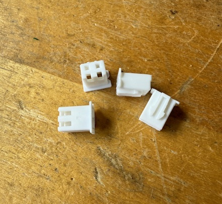
I also needed the "shells" (not sure what to call them) into which you shove the pins--I got these from Tayda.


...the crimping tool:


I couldn't get the exact tool in this video, but these Engineer Precision Connector Crimping Pliers were Amazon's choice, looked just like what is in the vid, and worked great. Hope the link here still works....


And of course, hook up wire (I used 24 gauge but I imagine 20 to maybe 26 will work) as well as some decent wire strippers.


PREPARING AND MEASURING THE PINS

The pin (this is a female version, the video shows males and females) have metal at the back that needed to be cut away:


Using diagonal pliers I cut away the extra metal on the right, behind the pin.


Next I pushed the rear fan on the pins until the were parallel and then measured their distance:

Came to 1.85mm, that meant I had to use the 1.9mm slot in the tool.


BTW: the female pins themselves are really small, I didn't wear magnification to do this work, but probably should have.


CRIM-PIN


Next I stripped the hookup wire, exposing about 1.5mm. This has to be done with a fair degree of accuracy. This was described well in the video at about :20.

Then I used needlenose pliers to gently affix the cable into the pin, otherwise the damn thing kept falling out of the tool before I could crimp. I found I didn't want to overdo things here, just a bit of pressure, to keep the pin in place, was most effective:


Then I oriented the pin with the tool--the orientation needed was not self-evident! It goes with the open end of the tabs into the larger slot of the tool:


Then inserted the pin and wire and crimped. Sorry, no photo....

When i was done, I could not pull the crimped end off the wire--it was really on there--all good.


Finally I shoved the pin into the shell. When it worked, I got a nice little click.


Repeated ad nauseum for the entire project. 


BTW, the whole process was exactly the same for me for Dupont connectors--smaller pins but same steps, using the 1.6mm slot in the tool:


The world is a happy place! 

 See you next time.

AS3364 Experimenter's Board--low parts count quad linear VCA's!

Readers: If you'd like to build the project featured in today's post, please go to PCBWAY's Community pages--gerber file; KiCAD 9 project/pcb/schematic/library files, a B.O.M., and more are here.  

You can also help out this site immensely by checking out PCBWAY using the link here. Thanks!

=====

When you put your Voltage Controlled Amplifier in series with a traditional ADSR you want the VCA to respond in a linear fashion, otherwise things can sound, well, crappy

The Irwin dual VCA from this previous post used 2 VCA's in series to get reliable linear response. 

Mike Irwin's design--I've built it many times now--sounds great, but required 2 VCA's for every audio or control signal I wanted to amplify or attenuate.

But what about a quad VCA IC with linear response out of the box? One that is affordable? 

That's the Alfa RPAR AS3364.


I built a simple experimenter's board for this IC, with buffered and clamped inputs for CV, so I could hear what it sounded like and avoid the terrible breadboard experience.

Works!


DESIGN

The secret weapon present in the AS3364: four log to linear converters, seen in its datasheet, one per VCA:

The AS3364 datasheet recommends 0-2V for control voltages, not commonly found in modular synthesizers....but getting my 5V control voltage signals to this level was easy--I used a voltage divider and MCP6004 op amp configured as a unity gain non-inverting buffer:

One of four buffers  

To power the MCP6004 op amp I used a simple 78L05 voltage regulator with a diode drop to give me about 4.3V DC:


This got 0-5V control voltages into a useful range for each VCA. The MCP6004 clamped incoming CV a little bit higher than its supply rails; I got a nice buffer to boot. 

I stole this clamping/buffering idea from Mutable (open source schematics here--take a look, highly recommended) who uses variations of this same circuit fragment in some of her designs.

THIS BLOG'S SPONSOR!


Before I continue, got to put in a quick word for this blog's patient and always helpful sponsor, PCBWAY. Once I get my circuit idea, I turn it into a .sch/.pcb and gerber file and send it off to PCBWAY.  They get it back to me super fast....PCBWAY fabricates at low prices (5x 2 layer boards 99mm x 99mm PCB's for about $5 US.....). 

PCBWAY provides a lot of other cool services as well: 3D printing and assembly, for instance.

Hats off to them, I am extremely grateful for their sponsorship of this blog. They do great work!


THE BUILD

Building the project was really easy. I used all through-hole because I had a bunch of 20K 1% resistors around; the BOM shows 30K but pretty much any matched values would have worked as long as I used the same resistors for all but R9.


Happiness is always getting new bubble wrapped PCB's from this blog's patient and friendly sponsor, PCBWAY.

Will it WFT (work first time?)


Only one way to find out-- 


tested with +/- 12V to see if I have shorts/magic smoke--nope. 


Worked and sounded great!

WHAT NEXT?

Alfa RPAR, the guys who make the AS3364, have a bunch of other interesting chips, the AS3365 (panner), the AS3363 (ring modulator and other functions) and lotsa other chip dookie.  

I would like to test all of those IC's out, but in the meantime the AS3364 might find its way into future designs due to its extreme simplicity. For instance, the EFM LFO2  (post is here) uses LM13700's as in-circuit VCA's; it would have been easier to have used an AS3364 IC.

Overall, an interesting chip for what we do. VCF's? Panners? Ring Mod? Sure. Lots of things I haven't thought up yet, and, "you can never have too many plain-old VCA's." 

See ya next time--Don't breathe the fumes.

Stereo Panner using the Irwin dual VCA

Readers: If you'd like to build the project featured in today's post, please go to PCBWAY's Community pages--gerber file (main board); gerber for jacks board, front panel gerber, KiCAD project/pcb/schematic/library files, a B.O.M., some wiring diagrams, and more, can be found here

The project also uses a small jacks PCB for the 3.5mm jack breakout, that project is here

You can help out this site immensely by checking out PCBWAY using the link here. Thanks!

=====

Hidee Ho boys and girls! 

Last time I laid out an Irwin Dual VCA, this time I wanted to put it to work.

I designed and built a stereo panner in Frac Format....


.....to replace a similar build from 2004 (?) which of course I didn't document.

Right one looks better?

The old panner was broken--its bias offset switches no longer worked, making the audio outputs cut in and out in some situations. 

Could I fix this 20+ year old module? 

Not easily--when I inspected the old design I found that the add-on board for bias adjustment was wire wrapped--I did this?

DESIGN

I didn't document any of my work back in 2003 but could recall how the panner was conjured.  

A quick sketch of the layout:


How it works:

Audio A+B is a mono input fed to normals: Audio A and B.  The Irwin VCA design can amplify and attenuate control voltages as well as audio, so the "audio source" can be any signal from DC to 18Khz and beyond.

Same idea for the modulation signal--single mono feeds 2 normals; plugging a 3.5mm jack into "A" or "B" overrides the normal. 

Each modulation signal goes through a portamento subcircuit and 2 buffers; each buffer has an optional offset voltage (1/2 of a dual contentric potentiometer on the new build; a 5V SPST switch on the 2003 design).  

One CV buffer is inverted; each buffer output feeds one side of a center tap pot (CT pot datasheet is here).  

I considered adding a mixer for a combined A and B out, as well as 180 degree inversion of one or both audio inputs, but that would have overcomplicated the circuit; I already have lots of mixers and audio inverters in my rack, so I figured I would just patch them as needed.


CONSTRUCTION


For S&G's here's a pix of the 2003 build. 

2003 circuit--Wire wrap?  really?

....in general the old module was built with (as my tech boss in the film business used to say) duct tape and snot.

Nice cold solder joints, Elmo!

I figured it would be easier to get new boards from this blog's faithful and ever-patient sponsor, PCBWAY, instead of reverse engineering then repairing my 20+ year old build--they always provide fantastic parts, and can assist in all your DIY needs, from 3D printing to assembly to metalwork and beyond.

You can greatly help this blog by checking them out: use the link here.


Back fast! 

In the shipment I got a "jacks and pots" board.....


.... and a small PCB for 2x dual concentric pots--a personal favorite component for saving front panel space....


....as well as a front panel:


.....I reused the Irwin Dual VCA from this previous post:


I used 4x40 standoff hardware to make modifications and fixes easier at this early stage of prototyping:


SMD AND JST


During the pandemic I found using 1206 SMD components was easiest for super-fast prototyping--counterintuitive, right? 

I often found myself wanting to change out parts, doing so with through hole parts was time consuming and occasionally destroyed pads on the PCB, even the super tough pads from PCBWAY, when I got really impatient. 

Find a previous post about my journey into SMD DIY here

I have also standardized (somewhat) on JST-XH connectors and hook-up wiring for building nascent prototypes. Skiff designs at an early stage of development leads to frustrating and hard-to-fix shortcomings, like pots needing to be turned counter-clockwise to increase volume. Nice to be able to rewire things!

The initial build went fast, fast, fast

I laid out the jacks-n-pots board in less than 45 minutes:


From here it was smooth sailing--like building a kit. I already had a DUAL SOIC VCA ready to go--read more about the Irwin dual VCA here.


Since the dual concentric pots mount at 90 degrees they needed their own PCB.


initial tests....


WFT/BISC


So did it work first time (WFT)?  Yes, but it soon croaked (BISC).

After taking an evening off--which oddly sped up troubleshooting, I came back to discover the problem was easily diagnosed: some of the 24 gauge wires I had soldered between boards were broken. As I tried to fix them, more broke, then fixing those, more broke. 


To ameliorate I came up with a simple bodge--using 100 mil edge connectors and shrink tubing on one side of each connecting wire:


..............which ended up looking like this:


It would have been more elegant to crimp JST-XH 100 mil connects to both sides of the jumper cables but at this early prototyping stage this workaround was good enough.

WHAT NEXT?

The 3 PCB's for the project--jacks board, front panel, and concentric pots board--could be laid out more efficiently; I had a few ideas for making modulation bias adjustment--needed in some cases for a smooth stereo pan at audio out--easier to tweak. 

So....I will create revisions of the 3 PCB's, rebuild this in the coming weeks, and, if there is love, post it all on PCBWAY's community site. 

I already have the "version 2" boards laid out. 

I figure they will WFT? We will see. Stay tuned! 

UPDATE 4-10-25: Yeh, the improvements are done, and it all works!  See the PCBWAY community site page here--up and running.


AI generated background (sorry)


 OK enough for now--see ya next time.