1J24B part II: Tube Based Audio Timbre Trasher and Experimenters' Board

From this previous post: audio bench experiments using the interesting, inexpensive, small, low voltage 1J24B pentode continue. 

What else can we use this miniature valve for, in our rack, our bench, and so on?

How about a timbre modifier? While breadboarding, I noticed that putting a capacitor between the tube's screen and ground seemed to distort the waveform found at the anode (the tube's "output").  As the screen voltage changed, differing frequencies were driven through the cap, causing odd waveform distortions you could see on a scope (to use US slang--we are "trashing" the signal--a "timbre trasher"?  Why/why not?).  

Breadboarding a 1J24B, with its tiny exposed wires, proved difficult, so last time I designed a 100mil breakout board for the tube and its power (post here, project notes with gerber is here).  

I could probe the buffered and cap coupled output of the single 1J24, and auditioned the prototype through my bench preamp/amp/speakers. 

To my ears, with all the buffers set up correctly, the design sounded a bit "filter like", maybe reminiscent of a 12db/octave VCF without resonance.  Cool!

But even with the 1J24B breakout board on my bench things got unwieldy. 

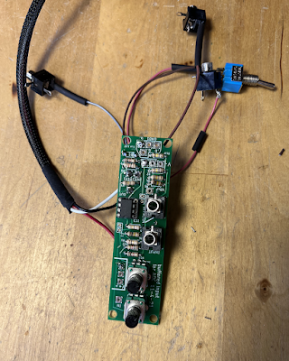
I figured a dedicated "tube trasher" PCB for further experimentation would help a lot. So I drew one up....

The PCB looks like this:


I got this fabbed by the blog's sponsor, PCBWAY, and here's the shameless plug: please help out the audiodiWHY blog and check them out.

The design pretty simple; the 1J24B is the center of the design, with a 30V cathode/plate voltage differential (an idea borrowed from Ken Stone's tube VCA, read more about that here--clever!)  Also a few op amps, since tube circuits like this require bias offsets and buffering, as well as 4 pots set up as voltage dividers between the V+ and V- rails.


The PCB is relatively large for the number of components used, making trace cuts, customizations, and/or offloading parts of the design to a breadboard, relatively easy and quick.


For fabrication I elevated the passive components somewhat, to make it easy to get a probe on one of the leads, or do modifications.


Then was a matter of populating whatever part of the board I felt I needed for the experiments. 

For the videos you see and hear below, I used 2 experimenter boards in series, with a 1uF AC-coupled feedback paths between boards' input and output buffers. 

Anyone who wants to follow along, see the wiring setup, get PDFs and Eagle files for design so far, and so on, should please go to the github repository here

You can also get a gerber for the experimenter board from PCBWAY's project page here.

Benchomania: I used "tall trimmer pots" to manually dial in the offsets, which I then noted; I will make a 3rd revision of this board soon with the values for the voltage dividers approximated with resistors, hopefully making the board less expensive to fabricate.


It works....


So far, this month's experiments have yielded a satisfying timbre shifter when 0-5V CV was applied to the first 1J24B's PCB screen, and an buffered and bias offset 1-2V P/P is applied to the grid, but the offset voltages seemed too sensitive for this to be fully practical, so this design still has a way to go; perhaps multiturn trimmers will have to be designed into the next PCB iteration along with some other tweaks?  Probably.

The video is a single experiment board, built and calibrated, being modulated by a 0-5V control voltage. The bias offsets used throughout are roughly documented at the bottom of the post here, but each 1J24B seems a bit different.  Again trimmers might be the way to go here.

For the incomings signal I used a 1-2V ramp wave with about -3V DC offset, from a Siglent waveform generator, but I had to try different things; the bias offset and amplitude of a source audio signal greatly influences what you hear at output, and too much or too little offset and amplitude for the source can make the entire output go dead--but once it's dialed in correctly, it works, but the "timbre mod" is pretty subtle and is more visible on a scope than with my ears. 


Next I wired 2 boards in series, and got the feedback going between the two. CV modifying the timbre comes from the output of an "LFO PRIME".  In this configuration, you can hear a bit more drama in the CV sweep.....if you want to learn more about what I've gotten to work so far, a wiring diagram, notes, PDFs etc., of the setup you see in the video below, is available via github, here.


Since 2V P/P saw wave gets nicely transformed into other strange shapes reminds me maybe a bit of "West Coast" work by Serge--back in the early 2000's I built a clone of the Serge Waveshape modifier, this design sounds a bit like that. So far, so good.

OK! For the next revision I'd like the 2 tubes and the buffer board to be reasonably small, but the design can't be SMD (yet) because too many design points are still being worked out. Maybe by next month I will have rev 3 ready to go? Stay tuned.

 Update 3-3-22: boards are designed, I should have them back from PCBWAY next week.  Assuming I can make it work, I will post the updated design in an upcoming post.


Bench Buffer--Protect Your Ard-weeno!

Continuing a previous post, here's a simple buffer/clamp circuit to make sure analog to digital converter (ADC) pins in your Arduino or other MCU don't blow up due to excessive over- or under-voltage. 

The design is simple: an op amp mixer with a zener diode clamp at its output. I have added a few other features as well. 

Elements of this design will show up in future projects, but if you want to build this into a module for your rig or bench, get wiring diagrams, gerbers, schematics, etc., on my github here; you can also have boards fabbed at my sponsor PCBWAY's Project Pages, here.


Without further ado:

Instead of testing the revised/fixed buffer-clamp PCB working, then resigning it to purgatory  in my "Prototype Fu" junk box, I created a simple frac module. Now I can use the clamp board on my bench and restrict audio or CV test signals to 0-5V by flipping the "5V clammp" switch. 

 The board in the previous post here had some mistakes;  here is the corrected, working schematic:


The result is a straightforward through-hole PCB that can be modified to suit most input/ADC buffering needs:


The board/module can be easily modified:

  • For ADC's that max out at 3.3V, change the zener diode (D1) appropriately.
  • The maximum offset voltage is normalled into the non inverting input of ICB3.  It's determined by R2 and R10.  It's set now to max out at 5V DC, assuming you are using a +/- 15V supply but different DC values are possible by changing out these resistors.  
  • I intentionally fed the offset voltage into IC3B pin 5; simpler would have been to introduce it in series with a 100K resistor to IC3A pin 2. I did this because in some projects I need to invert and offset a signal at input. I would place the incoming signal in series with IC3A Pin 1; R3 could be removed and the input signal presented there.
  • The output impedance is set by R8 and R9. These values can be adjusted and for most applications are not critical; R9 could in some cases be replaced with a jumper.
  • R12 and R11 set the range of the offset presented to IC3B Pin 5.  Larger resistors here will create a more narrow offset range.    
  • Make sure the voltage dividers use reasonably high value resistors (>10K), so as to not strain your power supply.
  • Hint: test your buffer before hooking it up to an MCU!

About the bench buffer: Let's add it to my bench setup. 

Some useless build photos:

PCBs sent fresh from this blog's sponsor PCBWAY. The shameless plug: Please help out this humble blogger and check them out....


Created front panel art with Illustrator

Testing the bench tool on the bench!

Front panel uses PCB material and "Mr Label" vinyl, see the posts here and here.


Junk box parts!  yeh!


Testing the fit....


"Seems working!"

 
Another month almost done--another module done. Next month I should be able to post a bit more frequently....tube audio stuff?  until then, don't breathe the fumes.

CON BRIO GATE: Boards Redesigned to eliminate fixes, trace cuts, bodge wires and other Problems. Works!

Boy Howdy! The ConBrio Gate Generator appears to be one of my more popular projects to date, based on blog post hits. However, the original schematic had a lot of mistakes.

Let's redo the board to fix the mistakes. 

Poof--DONE. Redesigned, new one worked without fixes on my bench.

To summarize, this is a +/- 15V synthesizer module that generates gate signals that speed up or slow down based on input data, think of a bouncing ball running out of energy, for example.  

Parameters can be controlled via gate and CV, and a degree of randomness is built in.

For the background on the module please see the original post here; you can hear what it sounds like here.


Better Never than Late: It took me about two years to finish redo/PCB fix. Thank goodness it's done! Get code, schematics, PDFs, wiring diagrams, BOMs etc. from my github, here. You can also see a "project" for this featured on my generous sponsor, PCBWAY's, project site, where you can download the gerbers and/or get the PCBs fabbed, here.

Let's build!!!!

Boards arrived from PCBWAY post-haste....if you need some PCBs fabbed, please help support this geeky blog and check out PCBWAY.


I chose to design 2 PCBs for this project--a main board for the nano and its buffers, and a board for PCB mounted pots and jacks. Hook up wire is used to connect the two.


Construction was straight forward, no real issues, although I didn't label the wirepads on one board to entirely match the other pcb, which was dumb. Maybe in a future revision? At this point probably not, but I have posted a wiring diagram on the github


Front Panel fabrication used a blank Frac 1U PCB and the construction techniques mentioned here and here:


Jacks were placed on POTS PCB, front panel fit, and then the components were soldered:


Next, I double checked the fit then soldered up the hookup wire:


Then I removed the front panel and cut and applied the vinyl label:


Some touch up, clear coat, and other tweaks, tests, and by Gates, we have a decent looking and good working module:


About the redesign: The main "nano" board is more complex than it needs to be. For example, for the transistor buffer for "Rev in" input I used 2 3904 stages; one transistor would have worked along with some simple code modifications. I wanted to have an "inverting input" for "REV IN" on the front panel but ran out of room so it was omitted. This could be easily implemented down the road but would require more front panel space, something becoming hard to find in my ever growing modular rig.  

Also when I first powered this up to test I found that the output and inverting output seemed to lag a bit. The output should have gone from 5V to 0V immediately, but it was more like a few milliseconds for the 5V to make it back to 0V. I remembered that fet based op amps have this issue at times when in series with other CMOS pins, such as what you see on a Nano.  

An LM324/LM358, which has slightly lower input impedance, solved this issue, so that what I used.

Brio Con Leave oh: That's it for this post. I start a semi-lengthy vacation tomorrow, and I haven't had any time off for a really long time, so there might not be a lot of posts in January. But I'll be back. 


1J24B Pentode: Developer's board = VCA and Timbre Fun!

Vacuum tubes, or "valves" have always interested me; why in some situations do they sound so good?  

I nearly burned down the house building a 5 watt guitar amp many years ago. I soldered the power transformer in backwards. That put further experimentation on hold, but twenty years later it's time to get back to it.

The 1J24B pentode (the bottom thing, Elmo)

абсолютно! I found an interesting pentode in a Ken Stone design--the centerpiece of his tube VCA, here. The VCA uses a Soviet era tube, the 1J24B, which can be purchased on Ebay for about $1 each in quantity. It's ideal: small in size, works with relatively low plate voltage (25-30VDC), and looking at the popularity of Ken Stone's design, works just fine. 

To get started I had to understand more about triodes and pentodes since they are the cornerstone of most tube based audio circuits. You can read a lot about how tubes work online, for instance, this webpage.  I also found two exceptional videos from Uncle Doug, YouTube's lovable guitar amp/hot rod/friendly cats n' dogs repair guy: here and here.  These are required viewing, I think, and made me realize I had no idea how pentodes worked while I was building my 5W amp. For instance, I didn't know that 6V6's, one of my all time favorite sounding guitar amp tubes, isn't a pentode at all!

Now, after some study, I know--a bit more?  maybe. You be the judge.

Here is a summary of the components you'll find in the 1J24B pentode:


How it works, quickly: Electrons boil off the cathode when1.5VDC is present across pins 1 and 2; the grid moderates the electron flow; the screen tells the electrons to hurry up (or not), and the suppressor keeps electrons that have struck the anode from bouncing back into the tube's guts and causing problems.  

I am still not sure what pin "3" is for, it appears to be used to tie the tube's body to ground. If someone knows, comment below and enlighten me, because I couldn't find anything about that; in every design I can find it's tied to ground so ve con tierra--go with ground.

Powering a pentode can be tricky, but Ken Stone came up with a clever solution: use +15VDC at the anode, then - 15 VDC for the heater with two current limited diodes in series so the cathode sees the approximately 1.3VDC needed to operate; wire it up so the tube effectively sees about 29.3V from cathode to anode:

Note--In his VCA, Ken uses resistors before the 2 diodes, and puts protection LEDs in series as well, but it's the same idea....

Another tidbit: The 1J24B has a "directly heated" or "hot"  cathode, which means DC (not AC--DC!) is directly applied to the cathode; there isn't an extra filament for the cathode. This makes the tube smaller, I imagine, but also means if there is ripple in the DC cathode supply it will show up as distortion at the tube's output. For what I am doing, any ripple caused by an LED or Diode is OK, but for something really hi-fi, maybe not. In any event, I had not heard of this "hot cathode" idea before.


With the backstory out of the way: to speed up my pursuit of understanding the 1J24B vacuum tube I created a "developer's board".  If you want to follow along you can download the gerber, BOM, EDA files, and so on, for the PCB used in the post you're reading right now, from my generous sponsor, PCBWAY's project site, here.  

Shameless plug: Please help support this blog! check out PCBWAY if you want to get a few 1j24B boards fabbed...or whatever else you're working on.


The idea: break out the floppy, easily tangled, easily shorted, frustratingly exposed bare-ass wire strands that come out of the 1J24B's butt to 100mil pins soldered to the side of a PCB. The diodes and resistors for power are soldered to the PCB, and there are some jumpers to change the basic power setup as needed.  For my build, I used R2 and R3 at 1.5K, and jumped J1, J2 and J3.  R1 and "anode jump" were omitted.  


With the 1J24B, resistors, diodes, and jumpers soldered in place, it's easy to put the 1J24B on a breadboard and start messing around.


Let's Go Get Kenned: Looking further into Ken Stone's VCA, which from bench tests looked more like a voltage controlled attenuator than a high gain amplifier, the fundamentals come into focus. 

With the cathode seeing about 1.3VDC, audio goes into the grid to moderate the electrons flowing; offset CV is applied to the screen to adjust gain, the suppressor is tied to ground to keep things sane, and the output at the "plate" or anode is capacitor coupled, removing the relatively huge DC offset that the 1J24B needs to function. 

The rest of his circuit uses op amps to condition the various signals to work well with the tube. At the end of the day, it's pretty simple, but of course you have to get it right for it to work at all.

Here are the voltages I saw at the bench. Feeding the cathode with about -13.5VDC across its terminals, the plate voltage could be anywhere from about 10V to 15V to get the sine wave to pass with minimal distortion. The anode inverts the incoming signal, and we see a 11-12VDC offset at output. Thus, capacitor coupling and buffering for the VCA output is essential; the tube itself adds very little distortion if set up correctly.  


From here I could present a sine wave at the tube's grid and out came a decent sine wave at the anode.  Incoming CV moderates the amplitude of the output sine wave. So far, so good!


If a tube VCA is your thing, take a look at Ken Stone's design for sale (here). 

But I wanted to see what else I could do--experiment time!  

It didn't take long to come up with a 1J24B based timbre changer or VCF, I am not sure what this really is:

I benched that with breadboards:


I haven't dug into this too much yet, but to me, the screen allowed only certain frequencies and harmonics to pass through, due to the .1uF cap, which caused odd distortions to the waveform at output--a 50% square wave ended up like this for instance:


The waveform at output was adjustable by changing CV and/or input audio DC offset and/or the 50K pot you see above. Fascinating! 

Testing: if you are getting little or not filter sweep, you may have a short somewhere. Check your voltages: you should see about 1.5V between the cathode pins; the grid signal should be AC with a slight DC offset (maybe -2 to +5VDC), while the screen voltage varies based on the CV input.  If you don't, say grid offset is close to -15V, you may have a short in the tube or elsewhere.  

Also I noticed that with a new 1j24B I saw about 30-100ohms resistance across the anode to cathode pins (1-2).  There was no other resistance I could find between the other pins.  If your tube out of circuit tests otherwise it may be problematic.

This might be the beginning of an interesting circuit, so I created a 1J24B footprint in Eagle:


In the copious (not!!) amount of time I have between now and the New Year I hope to refine this idea  by creating a design and PCB for a 1j24B timbre trasher. What would 2 of these circuit fragments sound like in series?  In parallel?  Can vactrols be used for the 50K pot?  Can you tie the output back to the input for--who knows? 

The usual....hours of fun.  Update 2-13-22: a timbre modifier design works on the bench, see the post here.

OK that's it for now. Pretty long post. If you are getting presents for the upcoming holidays, I'd suggest going tubular. Until then, don't breathe the fumes.