Hello Again!
A few posts ago I got an LFO working based on Atmel 328P and some Embedded C Code. The module (post here) works, but uses four--count 'em four--thru hole PCBs, electrical tape, plenty of "temporary" fixes, and a heapin' helpin' of elbow grease.
I know from previous experience that these butt sloppy modules stop working, or worse.
I can do better!
OK, let's build this module again but this time with higher quality.
I will also add "BOWAL" features (creating bias offsets at the inverting op amp inputs) adding much needed craziness to the module's incoming and outgoing signals--for more BOWAL see the previous post here.
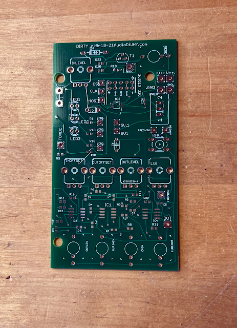 |
| The SMD board and solder mask for today's build is courtesy this blog's sponsor PCBWAY. Please check them out and help support future geeky posts.... |
Wham BAM! The new design is already back from PCBWAY. that was fast!!!!
I mostly chose 0804 SMD parts for this build, smaller than I've used before. Then I built the "analog" board using the same stencil and hot air process you can read about here.
 |
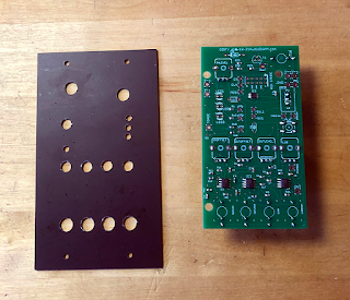
| I make front panels from PCB blanks, even before a newdesign tests working, to make troubleshooting somewhat easier. |
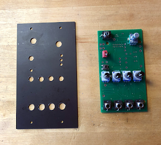
OK with all the components soldered in it was time to test.
Did the analog board work first time? Nope. The input and output buffers passed nothing through to the PCB mounted jacks. However the portamento sub-circuit worked the first time....it was time to troubleshoot!
I'll post the schematic once the build is finished......
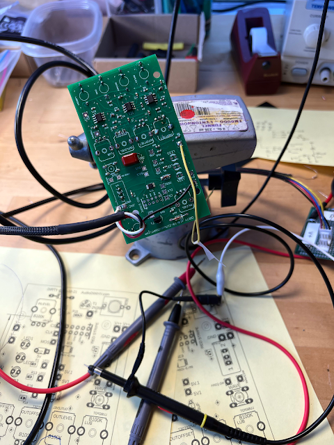 |
| Make sure you have a steady platform from which to probe, solder and fix. |
This design used six op amps stages for signal conditioning. Analog signals can swing rail to rail, but our 328P microcontroller only likes to see 0 to 5V.
How do we make sure nothing blows up?
Op amps!
I'd be surprised if anyone following this blog doesn't already know a lot about this component, but just in case, a series of posts about how op amps work and their primary applications begins here.
These fundamental ICs are a miracle when they work, but can drive you crazy when they don't; for a beginner they can be difficult to troubleshoot.
So.....Here are some tips I've picked up from other techs that I used to get the analog board's op amp stages fully functional:
- First--As always, don't guess! Don't shotgun! Don't brute force. Instead follow the wisdom of El Shango: follow your schematic and isolate the problem logically.
- BTW I get my kicks on Shango066. please fix things the way he does--divide and conquer.
- Using a scope or DVM, check that the op amp has the correct voltages at its VCC and VSS pins. If it doesn't, it won't work. Doh.
- Check that the op amp isn't wired up backwards (so, V- rail goes to V+ etc., chip was installed upside down, etc.). That can fry your op amp in a heartbeat.
- If you wire up op amp power pins wrong, even if the op amp doesn't smoke, you may want to replace the op amp...I know one tech who says you should do that every time you reverse power any linear IC, including an op amp.
- Draw a simplified mini-layout of the signal flow in and out of the stage under test, then check the signal flow carefully with a continuity tester.
- Check for continuity to the actual pins of the IC, not just its pad.
- For audio troubleshooting, consider using a ProbeMeUpScotty to follow your signal path to where audio stops--where the audio quits may be where your problem begins.
- If you are sending the op amp DC, use a scope or DVM to see where the problem starts in the same manner.
- Isolate each op amp stage from the rest of your circuit. I usually remove a resistor or cap between op amp stages or between an op amp stage's I/O and the rest of the circuit to do this.
- SMD tip: removing and reattaching small SMD resistors and capacitors has turned out (for me anyway) to be easier than dealing with thru hole removal/replacement. You need a steady hand, fine gauge solder, a magnifying glass, a fine tipped soldering iron, and of course a pair of zircon encrusted tweezers, but with the right tools it's easy and forgiving, even with really small parts.
- Once you're sure you've electrically isolated the op amp stage under test, apply a known good test signal at the op amp stage's input (inverting or non inverting, depending on your basic design).
- You should see your buffered output at the op amps output pin pad--use a scope.
- If you don't see a decent output (0V at output, output is slammed against V+ or V- rail, output has severe oscillations, horrible distortion etc.) then you know the op amp stage under test has a problem and needs more attention.
- Check and double check the parts in the stage's feedback loop and surrounding I/O for issues. Wrong value? Short? Open? Design mistake?
- You often can't scope the inputs of an op amp because they are virtual grounds. Damn! But you can sometimes use a neat trick to see what works and what doesn't.
- Here is an example of this--in this case, used to troubleshoot an inverting op amp stage:
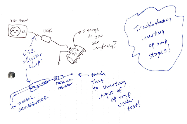 |
| Wire up a clip lead to a resistor blow a test signal through it. Now, touch the other end of the resistor to the inverting input of the op amp stage under test. If you now see your expected output (inverted of course) on your scope, you know the op amp chip itself is OK and its inverting feedback loop is OK too. You have further isolated the issue to the signal feeding the op amp stage under test. |
- Once you've fully isolated the issue look carefully for cold or bad solder joints, shorts, opens, a wildly incorrect part value, a stupid mistake in your design, and so on. It's almost always an easy fix but only once the problem is isolated.
In my case, I found 2 problems: a resistor that was shorted (I flowed too much solder below it) and an inverting op amp input that wasn't fully soldered down (probably too little solder paste).
At the end of it, I had a working analog board. The "minimalist" Atmel board design for this module is almost unchanged, so hopefully the rest of this build will go smoothly....and its code is already written and works. Yeh!
BTW, I may have hit upon the analog input buffer circuit fragment that I'll use in many future designs. I use this fragment to feed analog signals to analog to digital converters (ADC's); it's simple, has a reasonably low parts count, and gives me good control over many parameters that need to be adjusted before the signal is fed into our MPU's ADC.
Here it is:
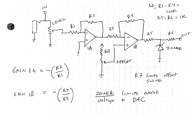 |
| Oops should read "limits overall voltage to ADC". |
This sub-circuit has the ability to limit the overall buffer voltage output (Zener), each gain stage (R1-R4), the output impedance (R5, R6 plus next stage's load characteristics), the bias offset (R7, pot), as well as attenuate the incoming signal's overall amplitude ("Level").
This is the fragment I am using for the post's analog board ADC input conditioning. How will it perform? Next post I will marry this analog "Pots" board to the MCU. Update--done! Works!! go here. See you then I hope! Stay safe, tune in and turn on.


No comments:
Post a Comment