
UPDATE 5-18-25: updated what you read below for Kicad 9.
The "ditch Eagle for Kicad" post is turning into one of my most viewed.
There, I discussed Kicad Version 7 importing most Eagle data into a new Kicad Project but not all of it.
Good news! With Kicad greater than V7 all the data needed for a new Kicad project can be imported from Eagle--hugely beneficial for anyone ditching Eagle for Kicad.
I felt the import steps deserved their own post, if you find this information useful well there you go....
However, if you have no need to import Eagle data into Kicad your time is arguably better spent watching these guys--have at it.
GETTING STARTED
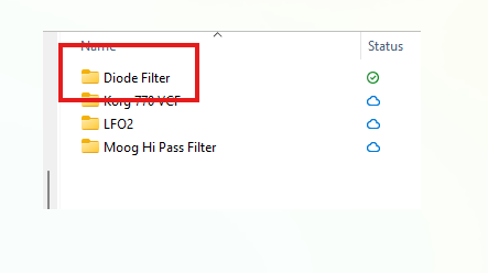
For this example I imported an EFM Diode Filter from Eagle to Kicad. I decided to call it--unimaginatively--"diode filter".
With the new project name in hand I made copies of the .sch and .brd files I needed to import; I left the original Eagle directory content as-is. This step was optional but I felt helped keep things better organized.
I created a new directory in my Kicad root folder called "Diode Filter"
....and a folder inside called "source files from Eagle".

Then, I pasted the copies of the Eagle .sch and .brd source files into this new directory.

In the same "Diode Filter" folder I also created a blank directory with the date--"Diode Filter 5-18-25"

LET'S IMPORT!


Viola! A PCB!

 |

EDITING SYMBOLS AND FOOTPRINTS
- Creating Courtyards. Footprints imported from Eagle didn't have them but Kicad wants 'em as a best practice. Courtyards for imported footprints have to be created by hand, so what the heck, I often edited the imported footprints and added them. Not technically necessary I figure, but, if I copied items from the imported project into new projects I figured courtyards were a good to have.
- Making Eagle fonts Kicad friendly. Kicad wants footprint fonts to be .8mm or larger. Imported fonts from Eagle can be smaller.
- Easy fix: I edited the footprint with the offending text, selected the text causing DRC issues, hit the magic e key, and changed the font width and height to .8mm or greater.
- I saved the footprint.
- Then, I reimported the updated footprint from its library into the PCB.
- Silkscreen madness: Eagle allows overlaps of silks and other silkscreening oddities that its default DRC doesn't catch but Kicad's does.
- To ameliorate: I edited the footprint, getting rid of or relocating silkscreen artwork that was causing Kicad's DRC to throw errors and warnings. I saved the updated footprint to my custom Kicad footprint library then reimported the updated part into my design.
- Pin name Changes: this seems obvious but I missed it at first.
- For my own edification: I should never expect pin assignments from Eagle to match much of anything in Kicad.
- Using imported footprints and symbols in a single imported project worked, but as soon as I used the part in a different project things sometimes broke.
- Meaning: traces to cathodes went to anodes, traces to transistor emitters went to collectors, traces to a pot wiper went to something other than a wiper--all bad news.
- Modifying symbols and devices from Eagle to work universally in Kicad required a bit of forethought and elbow grease. Diodes in Kicad needed pin 2 for anodes and pin 1 for cathodes, for example, as this seems semi-standard for Kicad.
- I found I needed to carefully examine imported footprints and symbols from Eagle if I wanted to make them part of my custom libraries, then edit them to make them work for a given future design. No easy fix for this, I had to do this extra labor or not use an imported Eagle footprint beyond its initial project.
- (BTW: for me--everything I think might be useful for future projects goes in my github custom footprint and symbol repos--e.g., my footprint custom library can be found on Github--here)
 |
| An symbol directly imported from Eagle. The pin name P$3_SLEEVE is useful for the imported project, but I found for other projects it was a good idea to change the pin designation. To this end I imported this jack symbol from Eagle into my custom symbol library, then changed the pin number to "G" to conform to Kicad's conventions. |


No comments:
Post a Comment