FPGA's 2025 Part II: Lattice/iCEcube2

Hello again, continuing on my quasi-annual attempt to get started with low cost Field Programmable Gate Arrays, or FPGA's. 

How will I do in 2025?

Last post I installed a Windows toolchain for Altera/Quartus; I read that offerings from Lattice Semiconductor are a bit more DIY/hobbyist friendly. Let's find out.

Nandland Go Board, sporting a Lattice FPGA chip


WHICH LATTICE-BASED DEVELOPMENT BOARD?

I already owned a couple of Lattice FPGA based boards: "TinyFPGA BX's",  hardware and their open source toolchain are covered in this previous post.

As far as I could tell BX boards were no longer being manufactured, also, I guessed that Lattice's software might be easier to get going vs. open source software I used to program the TinyFPGA's. 

After research: fingers pointed to Nandland Go Board as an affordable way to get started with Lattice FPGA's.....bought one!


TOOLCHAIN

The lower-end (read: less expensive) Lattice FPGA chips are programmed or "designed" using Lattice's iCEcube2 software. 

An Aside: Lattice almost removed itself from the DIY/student/hobbyist FPGA world forever (smart move? How much money do we spend on this stuff compared to these guys?) by raising license fees for IceCube2 from free to more than $470USB. 

Fortunately Lattice changed its mind, and iCEcube2 is available again using the five finger discount; we are back in business.

I followed the page here to get the toolchain going. Conclusion: Nandland's one-stop online resources (tutorials, purchasing, videos, more) made things much easier to get going versus Quartus Prime and Altera. Their "getting started" video and webpage (here and here) were invaluable; I went from nothing to blink in about 2 hours.

How I got iCEcube2 for free:

I had to create an account on the Lattice Semi page: here.

Then I emailed the Lattice Licensing dudes (lic_admn@latticesemi.com) with the subject "New iCEcube2 License Request" from my audiodiwhy email. I sent the email on Saturday. 

I was a bit surprised that the following Monday, yes, I got an email from Lattice Semi that had a serial number in it. 

With that, I went back to a Lattice website page (here) to turn the serial number into a license (*.dat file). Lattice emailed the file to me, I saved that on my Window 11 system's hard drive, then used it complete the installation of iCEcube2.

NOW--A WORD FROM OUR SPONSOR

I haven't crafted any audio projects yet using an FPGA, but when I do, I will run, not walk, to PCBWAY to get the boards--might be 4 layer?  They have been instrumental in helping get my projects working and they will take great care of you as well. 

If you need injection molding, 3D printing, assembly, and a lot more hit 'em up: 

You can also help out this blog by checking them out here

Back to today's topic....

ICECUBES (2 of them) in YER TROUSERS

During the iCEcube2 installation I had to enter the MAC address of my windows system (start > run > cmd > ipconfig); everything else was straightforward.

iCEcube2 did not have a built in programmer. As per the Nandland tutorials, I had to install the Diamond Programmer Standalone (here).  Be sure to download the 50 odd MB Standalone programmer, not the 1GB+ Diamond software zip. You only need the former.

I downloaded and installed the Windows title:


I also downloaded the FTDI Windows driver for the Go Board, here. I installed the driver for Windows 11 using all defaults, a reboot wasn't necessary.

All in all--pretty easy.  

Next: a few screenshots that might prove helpful in 6 months when I forget all this.


When creating an iCEcube2 based design, the program will save your critical .bin file--the binary file needed to blow into the FPGA--to god-only-knows where. Wait, I know where! [project]\sbt\outputs\bitmap.  

The Diamond Programmer needs the changes in red above to work with the Go Board....


Then: "device properties" need to be set for the Go Board. Note--"Device: M25P10" did not match what is shown the Nandland blink project video, but the M25P10 setting worked.

Thankfully, you can save your programming configuration as an xcf file. That way you don't have to configure the standalone programmer every time you have a new project. 

Cool!


CODE

To test the toolchain I used the .v blink code from the Nanoland site.


module Switches_To_LEDs

(input i_Switch_1,

input i_Switch_2,

input i_Switch_3,

input i_Switch_4,

output o_LED_1,

output o_LED_2,

output o_LED_3,

output o_LED_4);

assign o_LED_1 = i_Switch_1;

assign o_LED_2 = i_Switch_2;

assign o_LED_3 = i_Switch_3;

assign o_LED_4 = i_Switch_4;

endmodule 

I uploaded it using the instructions from the "getting started" tutorial--here.  

It didn't work at first, but I ran through the steps a second time and viola:

BLINKORAMA?

I reached Newbie Nirvana: press SW1 through SW4, the damn thing blinked.

Boy Howdy!

What next? There are low-code/no code options, like Icestorm (here), and, maybe I can use AI so I don't have to learn Verilog. I also found an interesting video about using Logisim Evolution (previous LSE post is here) to generate code from schematics: click here.

But first I have to come up with a project for my nifty FPGA boards. 

Maybe some sort of all-FPGA Lunetta thingy?  

We will see. See ya next time!

FGPA's 2025 part I: Intel/Altera/Quartus

Hello there, it's a new year, and I am jumping back down the FPGA rabbit hole:

Tesaric DE10-LITE. The URL for the CD, on a sticker glued by the manufacturer to the board, 404's. Sorry.

I last worked with FPGA's a couple of years ago almost to the day (post here)

This time I wanted to see if I could figure out how to use an FPGA for accurate data acquisition (the frequency counter project/multiplier, for instance: here).  

I got out my tinyFPGA BX for this but soon found out it's listed on Digikey as "obsolete" and not currently for sale.... 

Hello? It's only a couple of years old but, whatever.

Digging into alternatives, wow, the FPGA market is figure 8 trailer racing: 

In a nutshell: the FPGA landscape apparently changes more quickly and more often than my chonies.

Older, lower density FPGA's are being phased out:

I bought this Altera Cyclone II development board a few years ago for next to nothing, but recently discovered that the current Quartus programming IDE no longer supports it. Sorry. I might be able to get an older version of Quartus working on an Windows 7 VM and revitalize this dinosaur? 

Regardless, as a birthday gift to myself, or maybe because I love punishment, I bought a few newer FPGA offerings and will try to get their toolchains going in the next few posts.  

This time it's Intel, Altera, and Quartus. But first.....

PCBWAY--THIS BLOG'S HUMBLE SPONSOR

No matter what FGPA I end up using, if I have to fab up a board for it, my stop will of course be my sponsor, PCBWAY.  They manufacture small quantities of PCB's for very affordable prices and work and ship very quickly. They also do injection molding, 3D printing, assembly, and a lot more. You can help out this blog by checking them out here.

A QUARTUS LOW?


Quartus Prime Lite Edition is the free offering from Intel (Wait--Altera? or these guys?) you can use to program supported Intel FPGA's.

As far as I can tell, Quartus Prime Lite is the same software with the same features as the >$2k USD  licensed versions but only supports Altera's current line of lower density FPGA's. 

Good enough for what we do? Probably, yes!

I downloaded and ran the 28MB SFX installer for Windows: here. Some how-to videos such as the one here demonstrated downloading tricks needed to get Quartus Prime Lite to work for free, but nope, the single file linked above pulled in necessary files and the install was simple. 

Best of all--no license was needed! 

Warning: As mentioned above, the FPGA scene is always changing fast, so who knows when the links in this post will break....if you want software so you can program your FPGA, get it soon!

For hardware: after some research, a good bang-for-the-buck option supported by the current version of Quartus Prime Lite is the Tesaric DE10-LITE.  
 
There are less expensive Altera options, but for now, I wanted to make sure I could get the toolchain to work and a lot of documentation pointed to Tesaric.

The video I followed to get the toolchain up and running is Olawale Akinwale's offering here

This was a helpful video, but Olawale showed me how to do something wrong before showing me how to do it right--educational, but, time consuming. You might want to watch the whole video before attempting to get your FPGA board working.

For Verilog code I used the same .v file the content he used:

module lab1_1 (SW,LEDR);
input [9:0] SW; //slide switches
output [9:0] LEDR; // red LEDs
assign LEDR = SW;
endmodule


A few things not mentioned in the video:

  • The USB-Blaster driver did not install correctly on my windows 11 system during the initial Quartus install. 

To get that going I ran the DPINST.exe program that was installed along with Quartus. On my Windows PC I found the app here: C:\intelFPGA_lite\23.1std\quartus\drivers.  


I found other videos and forum posts saying to fix this issue use Windows device manager--but for Windows 11, no, that didn't work.  Running DPinst.exe fixed things; I can now see "USB-Blaster [USB-0] in the "hardware setup" dialog.

  • To blow your verilog code get into the firmware of the dev board--and not have your work wiped out each power cycle--the Programmer UI needs to be set to run the .pof file and "program/configure" needs to be set as you see here:


Beyond that the video was spot-on.

After uploading to the FPGA deb board, and solving the issues above, each slide switch turned on or off its corresponding LED. 

It worked! Cool!!! 

str = 'F' + str.Substring(1);


Say what you will about Intel, Quartus is a super powerful piece of software.

Next, I found out that you can do low code/no code Verilog development using its "schematic" feature. Video is here.  

Using that I drew up a few AND gates and converted the schemo into verilog code:

"File" > "Create/Update" > "Create HDL Design File for Current File" (I had to have the .v overarching project open for this export to work).

I got this:


module lab1_3(
SW0,
SW1,
SW2,
SW3,
LEDR0
);


input wire SW0;
input wire SW1;
input wire SW2;
input wire SW3;
output wire LEDR0;

wire SYNTHESIZED_WIRE_0;
wire SYNTHESIZED_WIRE_1;


assign SYNTHESIZED_WIRE_0 = SW0 & SW1;

assign SYNTHESIZED_WIRE_1 = SW2 & SW3;

assign LEDR0 = SYNTHESIZED_WIRE_0 & SYNTHESIZED_WIRE_1;


endmodule


QUARTOUTTRO?  QUARTUSTRO?  QUARTOJUMBO? 


Between these features and AI maybe I can do useful FPGA coding without having to learn a ton of Verilog.....

Obviously I have a long way to go here, but, figuring out this new toolchain was a lot of fun.

Next up I am going to look into current offerings for Lattice Semiconductor--thankfully, they are still around, haven't been recently acquired by a wig company, and in that they have some lower-end offerings and seem to care about the hobbyist and semi-pro community, might be a better fit for DiWHY.  Update: done, Lattice FPGA hardware and a free toolchain work--post is here.

We will see.


EFM LFO2--Old Skool Fun


Readers: If you'd like to build the project featured in today's post, please go to PCBWAY's Community pages--gerber file (main board); gerber for jacks board, front panel gerber, KiCAD project/pcb/schematic/library files, a B.O.M., follow this link to get GitHub simulations for the design and more.

The project also uses a small jacks PCB for the 3.5mm jack breakout, follow this link.

You can also help out this site immensely by checking out PCBWAY--here. Thanks!

=====

I needed a break from programming, MPU's, logic, and whatever else, and stumbled upon a cool LFO design from EFM ("Electronics for Music"). 

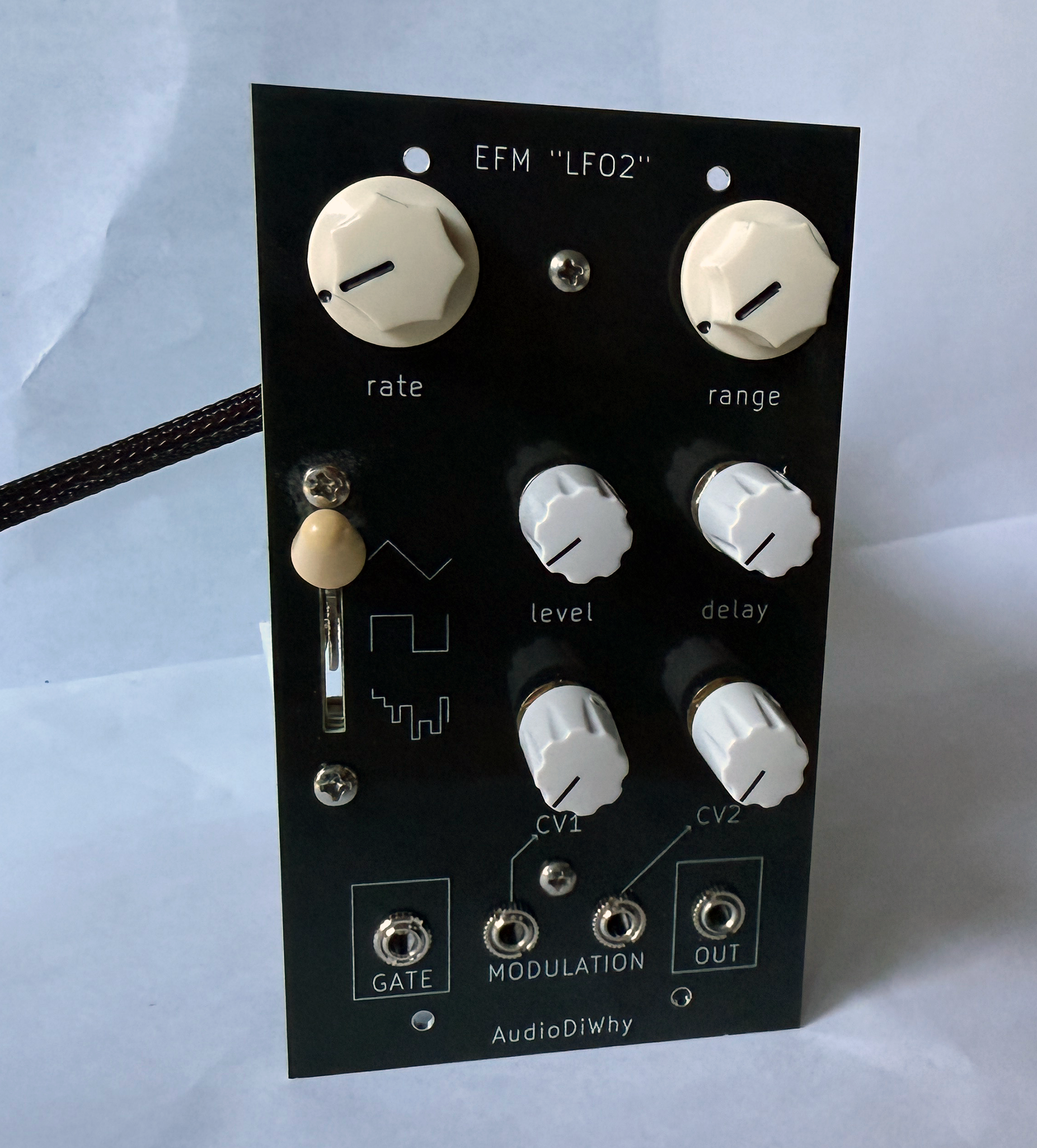
I decided to build it:


To further break with past Eurorack projects I built this "EFM LFO2" in PAIA's Frac Format, giving the build a large format look and feel: +/- 15V rails, panel mount potentiometers, and hookup wire.

I had forgotten how much fun it was going old-school--I could try out different things, slap in modifications, and quickly recover from the stupid mistakes.  

DESIGN

LFO2 caught my eye because of its extensive use of OTA's and the different ways current was passed to the CA3080s' amp bias pin 5. 

Using Falstad I simulated the different sub-circuits that fed  bias current to the circuit's OTA's: get the simulations at GitHub by following this link

Falstad sim for the LFO delay sub-circuit

If you want to learn more about how to incorporate OTA IC's into your designs a great resource is Thomas Henry's book "Making Music with the 3080" here; highly recommended.

The circuit also incorporated a CD4007--an interesting IC, 6 MOSFET in a 14 pin DIP. 

It clamps and buffers an incoming gate signal to control the LFO's onset delay--yep, CD4007, an IC with 1001 uses.

Overall: LFO2 combines EFM/Tom Gamble's signature economy-with-coolness--it's a clever circuit that demonstrates Mr. Gamble's considerable skill as an analog audio design engineer.

The project used 3 PCB's: a 3.5mm jacks board found at PCBWAY's community site here; also a front panel, and a main board--find the latter two in this PCBWAY community project.

I copied the EFM schematic into Kicad 8 and laid the main board out on a 99 x 99mm PCB.

You can get a 99x99 board from my sponsor PCBWAY dirt cheap: 

GO PCBWAY!

Shout out to Serene and the good folks at PCBWAY for help getting this project off the ground. I use them for all of my PCB fab and have also counted on PCBWAY for metal work, 3D printing, and assembly. They do all this and a lot more.  

They always do great work, are extremely affordable, and ship super fast. Please help this blog and check 'em out..

THE BUILD

I employed the same design and fab techniques found in this previous post, but employed a SMD stencil (a good video for using stencils is here--go to 38:10--showcasing the technique used for this LFO's build), stencils are available from PCBWAY of course.

IMPORTANT! For what we DIYers do, pick the "non-framework" option when you order your stencil--for instance, at PCBWAY the order choice looks like this (I figure all fab houses offer this option):


Happiness is a batch of new PCB's:

3 boards and a mask....

The build went  quickly, but of course didn't work first time (WFT). 

Here are a few useless build photos:

To add to LFO2's old-skool vibe I used JST XH connectors, hookup wire, and a Stratocaster 3 position switch. Fender Stratocaster switches are a standardized part, with lots of clones for sale; any decent Strat 3-position pickup select switch should work for this project.


I didn't have a .005uF (5nF) 1206 cap so I stacked 2 2.2nF 1206 SMD caps, which was surprisingly easy to do, I soldered on one 2.2nF cap, put the other on top, and reheated. 


I used DIP IC's, not SOIC. The project is a mix of both. 

"Wires R us"


MISTAKES, I'VE MADE A FEW

But then again too few to mention? Nope. Lots to mention.

I misread the schematic; the "range" pot to the left is a 10K trimmer but no, I made it panel mounted.  

So....I soldered a 10K 25 turn trimmer into the JST footprint (perfect fit, I got lucky).

I thought a first the circuit didn't work at all, but once I turned this "cvrange" trimmer down pretty far things started to work. 

But...now I have a big drill in the front panel ("Range") that doesn't need to be.

I fed a 50K "range" pot to pin 3 of the EXT JST.  Feeding this range pot was V+ from the Euro 10 pin power header; GND was provided to pin 1. I had to add a 10K resistor between the wiper and EXT to make sure if the pot was set fully counterclockwise--to ground--the +15V supply rail wasn't sent there as well.

This meant when nothing was plugged into MODULATION CV2 the range knob provided 0-15CV to the OTA controlling frequency.

If I revised LFO2 I'd put +12V or +15V or whatever to the normal of one of the mod pots....but the modification to fill the useless "range" drill worked. 

I also had a considerable amount of trouble remembering that when I looked a potentiometer from behind its pinout is 3-2-1. From the front it's 1-2-3. I had to re-solder a few pots.

I also mistakenly plugged one of the pots into the EXT JST during testing. The EXT JST is for normaling this module to others and could be omitted. This mistake created some very strange behavior while testing until I unplugged the errant pot.
 

MODS TO THE EFM DESIGN

Only one: The random voltage output's bias offset increased with the LEVEL pot's settings, which some synth nerds might like, but I didn't.  

I put a 10uF cap in series with the 3 position switch input for SQUARE, which knocked its DC offset output to ground regardless LEVEL's setting. 

The 10uF cap turned the random signal into not-quite-a-square-wave, instead, more of a randomly changing, slightly saw-toothy square wave, but: good enough. 

Maybe even better, the cap adds an analog vibe to the LFO's random output.

If I do another revision of this module I will add the 10uF cap to the PCB design.

PERFORMANCE

This is a cool LFO with a early Roland modular  feel. The delay goes from 0 (no delay) to maybe 20 seconds. The main issue is that some level settings, which control the overall output amplitude for all the LFO's waveforms, distort the triangle wave and can push the square wave output to a DC rail voltage. Not sure how to fix that quickly, but I can live with adjusting the LEVEL pot to get the output I want. 

The frequency at output goes from slow < .1hz (with sufficient negative CV frequency modulation) to a nice fast-modulated sound--satisfying!

Overall, this was a really entertaining project, and I needed a fun build after some not-so-fun builds. 

Going forward I may create more large format/frac/ with wires, guitar switches, pots, and whatever else. The guys in my synth geek group always like retro looking stuff--so, why not?

EFM/KORG770 VCF--BUILT: yes, WORKS: yes, SOUNDS: bad

Ahoy! 

This time, I wanted to refine the quick prototyping idea discussed midway through this previous post:

  • Minimal breadboarding--I hate breadboards
  • Hookup wires for fast modifications/fixes to switches, input jacks, and potentiometers using JST connectors 
  • Panel mounted hardware
  • SMD 1206 parts--easy to place, easy to change; heat the part up, remove it, drop another value in.
  • SOIC IC's
  • PAIA Frac Format--bigger than dinky Eurorack--not as rotunce as large format.

The idea: if I came up with something really cool I would port it to another format....Frac isn't dead, it just smells funny.

This time I put this workflow to the test with EFM's take on Korg's 770 VCF:

Frac me up Scotty? find a listing of all cool EFM designs here


 A real 770....could the 1999 VCF design from DIY pioneer Tom Gamble get me the sound of classic 700/770 synthesizers?  

I heard a B3 guy play a Korg 770 at a music festival a few years ago and thought it sounded--bodacious.

So I laid out some boards based on the EFM design, using KICAD, and off to PCBWAY the gerbers went.

THANKS TO THIS BLOG'S SPONSOR: PCBWAY

PCBWAY was super as always about turning around the boards for this project around fast! Instead of breadboarding it is always much less time and frustration to lay out KICAD designs and send them off to be made into PCB's. 

For this service, PCBWAY is always extremely helpful, super affordable, and fast! 

As always I got my PCB's right away, fabricated to perfection. And! PCBWAY can do a lot more: 3D printing, assembly, metalwork, injection molding, are all cake for these guys. You can get five 99mm x 99mm 2 layer PCB's for five bucks USD! 

Help out this blog and check 'em out here.

KORGANING.....

So with the cool PCB's back--did this project go?

The good news: the entire process of construction, populating the PCB's, and modifying them went much quicker than using through-hole, skiff construction, or breadboarding. 

Construction of the module in its entirety--this was not a super low parts count VCF--took about two hours. 

Since the quick prototyping challenge was met I could make simple changes to the EFM design post-fabrication fast, fast, fast.

The bad news: this particular 770 filter sounded really lame. 

Yeah, I made modifications and swapped in different component values trying to bring this filter into the land of the living; I banged away on the prototype for about three hours then gave up. 

PASS ON LOWPASS

I couldn't get LowPass section to completely block audio without greatly impacting its overall frequency response. 

So either I ended up with a constant "wah" or a modulated maximum cutoff frequency that was too low to be audibly pleasing. 

This drove me nuts.

Changing rail voltages altered this poor performance, so I tried doing wacky things with diodes to drop the power rails by .6, 1.2, 1.8 etc volts. 

This helped but I never got things to a place I liked.

Diode between rails and V--; instant drop from -15V to -14.3

The LP filter input brought the audio signal down at output about 16db (!); output amplitude got slightly better with a decent amount of resonance added; but amplifying the circuits output back to near unity with an additional op amp made the output too noisy/hummy/buzzy.

If I cranked the "Q" pot past about 80% I got horrible sounding distortion at output. This was not cool MS20 Daft Punk distortion: this was butt-ugly distortion. 

The bandpass setting, which I don't recall a Korg 770 having, sounding, well, oddly bad ("badpass"?)

The highpass sounded (almost) OK?  It might have made sense to ditch the LP and BP sections and just focus on that with some mods?  Well, maybe, but maybe not, the HP didn't sound that good.

Overall the filter had a feminine quality, was a Seinfeld low talker, and didn't punch; to me, it definitely didn't capture any of the je ne sais quoi of old school King Kong Korg.

FABRO-CATION 

However the fabrication workflow felt like a win and I might do it again.

Boards in bags from the blog's faithful sponsor, PCBWAY.  Even when my projects sound really bad these guys do really good. Help out this blog and check 'em out.

Project consisted of 3 PCB's: front panel, jacks board, and main board. Also a cheapo stratocaster guitar pickup selector to choose LP/HP/BP. Why not?

The jacks board is 4x 35RAP Switchcraft 3.5mm mono jacks, spaced 600 mil apart. This small PCB might find its way into other projects.

I used the SMD goo-n-tweezers + hotplate for the lions' share of soldering. Read more about this solder technique midway through the previous post here. This is the "before" picture: sloppy, right?


Ah! better! The goo-n-tweezers method is pretty forgiving since the parts center themselves during soldering. I had to solder wick one side of the op amp and resolder D2 by hand, other than that, all the soldering came out great.

Next I added the hookup wire and panel mount pots. I had everything right the first time, no pots where CCW was 100% , no input jacks hard-wired to outputs. 


KORG ME UP, SCOTTY?

So, where do we go from here? If I felt I could get anywhere near the cool Korg 7xx series sound with this VCF I would have kept working. But I wasn't on the same planet.

I put kicads, gerbers, libraries etc. on github: here.  

If anyone wants to fork this dork, or do whatever you want: do whatever you want. 

I also posted the jacks board (which i figure I will use in other projects) to the PCBWAY community site: go here.

I am going to strip this one down for its reusable parts and move on. This module's death may allow others to live.  

Over and out captain. See ya next time.

JTAG to SWD Converter

Readers: If you'd like to build the project featured in today's post, please go to PCBWAY's Community pages--gerber file, KiCAD files and a B.O.M. are here.  

You can also help out this site immensely by checking out PCBWAY using the link here. Thanks!

===== 

Hello again:

Another simple one!  

I use GDB to debug C based embedded system projects--I currently use a Segger J-Link EDU debugger with a JTAG interface:

Segger J-link EDU Mini

But! The development board I am currently debugging is a Raspberry Pi PICO that has an SWD interface:


JTAG is not difficult to turn into SWD, it's a "connect this pin to that pin" challenge.

However I got tired of fiddling with tiny fragile adapter cables so I whipped up a simple JTAG to SWD PCB; the focus of this post.


REQUIREMENTS

The J-Link EDU Mini's JTAG interface uses a 2x5 pin 50 mil pin header--1.27mm --extremely small--conforming to the "Coresight 10" JTAG pin specification


The Pico uses 3 x 100mil SWD pins for SWCLK, SWDIO (data), and ground:


The Segger J-Link EDU board, unlike Segger's more expensive debuggers, requires a 5V reference....there were may ways I could have gotten 5 volts to the adapter PCB, from a USB cable for instance? Or a battery? 

However I used wirepads and 22 gauge solid wire and connected a bench power supply for 5V; I may rethink this design choice down the road. 


DESIGN AND LAYOUT

Simplicity itself....took me maybe an hour to lay out the PCB in KICAD, very little thought went into design, perhaps it shows?


Did a very quick 3D check in KICAD....good enough--sure. Off the gerbers went to PCBWAY.


BUILDING/TESTING:


PCB's are back! Happiness is new PCB's from this blog's sponsor, PCBWAY. Please help this blog by checking them out.


Easy build. The SMD JTAG 2x5 connector was pretty small but I managed to solder it without needing my microscope.

For the Pico I used a 3 pin JST connector:

The more JST connectors I use the happier I get, they are inexpensive and extremely reliable. You can get them for next to nothing from Tayda.


To test I coded a simple C proof of concept program: "PrintRTT", which used the adapter board to bring printf() statements from the PICO to a Segger J-Link and then to my Linux system. 

Wired it up:
Pico needs power as well--use USB and/or 6V-9V and GND to pins 39 and 38. 


Worked--I dragged the UF2 file to my Pico and ran the Segger "JlinkRTTViewerExe" terminal app on my Linux virtual machine..

You can get the code from Github here

Instructions for using the Segger printf() overload and the Segger RTT app are covered in latter half of the post here and the Segger page here.

Adapter with a "stock" Pico....the red and black gator wires are 5V and GND from a bench power supply, needed to provide the JLINK with its 5V reference.

And to debug the rotary encoder experimenter's board....

The adapter board was a piece of cake and worked first time. Viola! No more fiddling with tiny fragile SWD cabling. 

I had a few ideas for improvements: clarifying the silkscreens and adding more diode protection.

But for now it's time to move on.  

I remain extremely happy with the Segger J-link Mini EDU. There are other PICO/RP2040 GDB debug options  (DIY "PicoProbe" and the offering here) but to me the Segger offers a good mix of simplicity, value, and useful software tools for a Linux-based toolchain.  

That said....I'm feeling a little tired of crafting embedded RP2040 projects and might fabricate a few analog EFM based circuits (will it work? it effectively frigging might?) in the next few weeks, a distraction.

And some analog design.  

Wait, analog? Math, breadboards, smoked parts. Sure, why not? Until then: don't breathe the fumes! 


Rotary Encoder Expermenter's Board: Improving the Hardware

Quick one this time....I have posted a few projects lately that incorporated a Raspberry Pi Pico, rotary encoder, and .96" OLED: here, here, and here. To make it unnecessary to breadboard the hardware, I posted an "experimenters board"--a development board to augment a RP Pico that adds a rotary encoder, an OLED, and a buffered GPIO output, and other enhancements.

Just now I updated the KICAD and Gerber files on the PCBWAY community site salient to the posts: here.


The 9-29-24 revision of the experimenter's board uses less components, incorporates the encoder debounce library here, superseding the less responsive CD4011 based hardware debounce discussed here

Good news: it all works.

Thanks to Wendy and the gang and PCBWAY for patiently providing revised me with PCB's. You can help this blog by checking 'em out. 

9-29-24 revision

To make sure the grounding issues I saw with earlier revisions was a function the PCB's layout, not the schematic nor code, I breadboarded the entire "dev board for a dev board":


The breadboard example worked every time, but some of the older experimenters PCB's didn't, so, for versions of the board prior to 9-29-24, I was fairly certain this was a hardware/PCB layout issue.

I thought trace layouts for low frequency audio wasn't terribly important--put things almost anywhere, throw in whatever traces you want--it will work--we are bottom feeders?

Wrong. Apparently the I2C traces (at the very least) needed to be treated with forethought.

Previously: more narrow traces....no ground pour


9-29-24 design improves that. 

I found myself putting the 9-29-24 assembly on hold for a couple of weeks, partially because I was tired of revising the board, and also having a feeling (incorrect, fortunately) that the 9-29-24 revisions would make things less reliable, not more.


Word of caution: 1306 128x64 .96 OLED's are everywhere but there appear to be 2 different pinouts coming from Shenzen: GND far left, and VCC far left.  

My design requires VCC on the far left--make sure you get that style of OLED if you build this project.

Spinning the rotary encoder advances or diminishes the counter on the OLED as expected. Every time, without fail. Thank goodness.  

Next: I have augment the code to create a user interface for the frequency counter....yes, I will get to that someday, but it means a lot of code changes.  

For now it's back to my day job--for better or worse the global pandemic is over.