Dirty Digital LFO--DONE!

Holy smokes (not literally--no smoke yet) this one was a lot of work.  


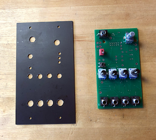
But it's finished; much improved from its thru hole build predecessor, and I am extremely happy with the results.

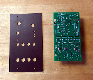
Left: Earlier Prototype of the Current Prototype....

Update 12-17-21: I created then posted a quick audio clip of the DDLFO. Go here.  About the demo: You can  use LFOs for most anything that needs modulation...but I wanted to show some of the odd  LF waveforms you can get from this strange device without a lot of  obfuscatory fanciness. So--The demo uses 2 Dirty DLFO's modulating each other with the lube out of one of the LFO's feeding a single VCO. That's it. I used a bit of multitracking and added reverb as as to not completely destroy your speakers, but this was the  simplest way I could think of to show you how a DDLFO module "sounds". 

There have been many previous posts about the D-DLFO up until now:

  • Leaving Arduino Sketch for Pure C: here (it was arguably easier to build a module of this complexity using embedded C vs. Arduino Sketch).
  • Minimal AVR board: here
  • Earlier DLFO prototype with simpler buffering (and less features): here and here.
  • Adding waveform reset via external interrupt: here.
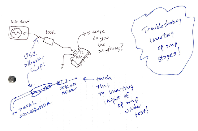
  • Fabricating and troubleshooting the SMD "pots board" for the build: here.

Also I want to thank my faithful sponsor PCBWAY for helping me realize the Dirty Digital LFO in its various incarnations. 

This was a tough fab, using 0804 SMD parts and intricate stencils. It's an advanced project. Their support and quick turnaround for the prototype boards was extremely helpful, so please help me continue to improve this blog and check them out.

Getting Dirty: Overall I am really happy I hung in there and rebuilt the original Dirty DLFO module to do more. 

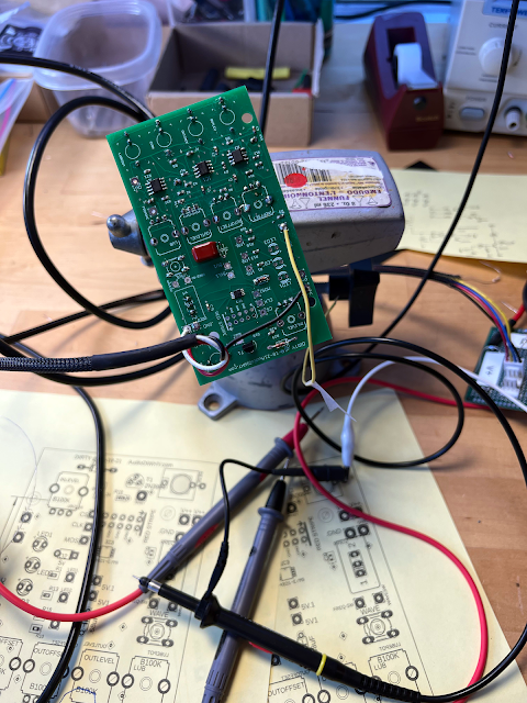
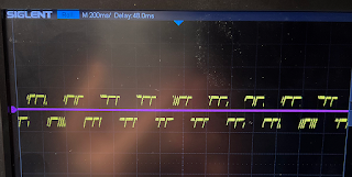
The waveforms you can create with it go from normal tri/sine/ramp/saw to bizarre. Check out a few scope shots. That's the wonder of DIWHY I guess, you end up with things that can be--different?


Generous lube makes the signal analog like....

Portamento turns tri into a sloppy sine. Good enough.

My stock portfolio?

Hebrew from an LFO? Oy!!

Swan Lake?

More Cowbell!

the path not taken?

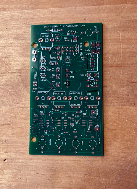
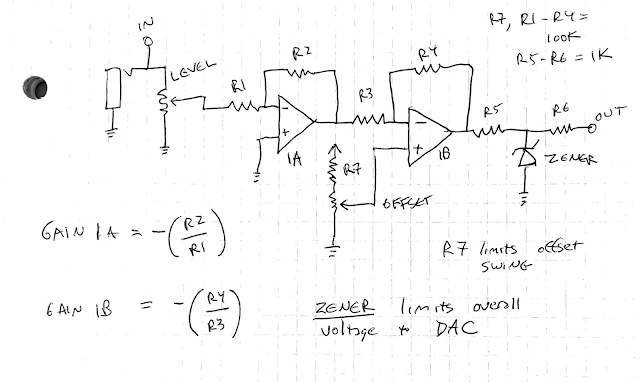
Using the Dirty Digital LFO: The module has two outputs: "Lube" and "Out", the former is the output  through a portamento subcircuit.  

The lube gets rid of the some of the digital grit which may or may not be what you want. 

There are 3 ways to change the frequency: the frequency pot at the top right, a slow/fast switch, and a 0-5V CV in. This is standard LFO stuff. You can set the output bias offset with the OFFSET pot (if I had more room I would have made the outoput voltage controlled, but enough features already right?) the WOMBO input mixes CV to the DAC out (see below); finally the CV bias in adds DC offset to the incoming CV in case a boost is needed.

What is a "WOMBO"?  I had to call it something....some of the strangeness you see in the scope shots is due to blasting CV in parallel into the DAC buffer output. We are not mixing the additional signal into the negative feedback side of the output op amp buffer, we are mixing it into what is normally used to set the bias offset (often tied to ground), here, treated as a mixer.  

I got this idea working on a friends' Ken Stone Dual Wasp Mixer, and thought it would be interesting feature to add to an LFO....it turned out to be the case. 

I had no idea what to call this input, so I chose 5 letters at random: "WOMBO".  There you go!

The PCB is wired for +/- 15V but should work on  +/-12V no problem; the PCB board I laid out accommodates a Euro power connector. 

As it's coded, the board supports 6 waveforms plus Sample and Hold:

  • Tri
  • Ramp
  • Square
  • Saw
  • Random 1 and 2 (CV controls frequency, or, CV controls frequency and randomness)
  • S/H (reset input, when it goes positive creates a sample of whatever is at the CV in and puts it at the output jack).

There is also a "Riley reset".  Hello? See previous posts here and here. This didn't work at first, after about 3 hours at the bench I realized that I had wired the interrupt to D1, but coded it for D0. Gotta love dumb mistakes. 

Since this interrupt starts the waveform over, you can get further complexity, such as turning a triangle into a saw, doing psuedo duty cycling of the square wave, and so on. Thanks to Max, Dave and the guys at BAM for insisting that I put this in.  It was a really good suggestion.

On to this post's useless bench build photos:


Showering off: Overall, this experience was AudioDIwhy at its best (for me anyway...)  

After hours of enjoyable and peaceful C coding, fantastically frustrating hours fixing and debugging the circuit, and much time spent swearing, soldering, wiring and having dumb bench fun, I ended up with a voltage controlled LFO that may be like nothing else out there--perhaps anywhere--if you have an LFO that can display psuedo hebrew-like characters on your scope, lmk--I didn't have one; now I do.

I feel I've come a long way since I was perf boarding dumb little op amp circuits and seeing if they smoked. So in spite of my psychiatrist girlfriend wondering about me and if everything is OK upstairs, I carry on--and perhaps this is a good thing. 

This was a pretty tough build, but if you are up for a challenge, you can get all the schems, files, gerbers, PDFs etc., from my github (here) as well as my sponsor PCBway's project page, here. Let me know if you come up with anything fun.

Here, now, I am happy.  Rock on!!!


Dirty Digital LFO Rebuild: SMD Analog Board--Troubleshooting Audio Op Amps

 Hello Again! 

A few posts ago I got an LFO working based on Atmel 328P and some Embedded C Code. The module (post here) works, but uses four--count 'em four--thru hole PCBs, electrical tape, plenty of "temporary" fixes, and a heapin' helpin' of elbow grease.  

I know from previous experience that these butt sloppy modules stop working, or worse.  

I can do better!

OK, let's build this module again but this time with higher quality.  

I will also add "BOWAL" features (creating bias offsets at the inverting op amp inputs) adding much needed craziness to the module's incoming and outgoing signals--for more BOWAL see the previous post here.

The SMD board and solder mask for today's build is courtesy this blog's sponsor PCBWAY.  Please check them out and help support future geeky posts....

Wham BAM! The new design is already back from PCBWAY. that was fast!!!!

I mostly chose 0804 SMD parts for this build, smaller than I've used before. Then I built the "analog" board using the same stencil and hot air process you can read about here.

I make front panels from PCB blanks, even before a newdesign tests working, to make troubleshooting somewhat easier. 


OK with all the components soldered in it was time to test.  

Did the analog board work first time? Nope. The input and output buffers passed nothing through to the PCB mounted jacks. However the portamento sub-circuit worked the first time....it was time to troubleshoot!  

I'll post the schematic once the build is finished......


Make sure you have a steady platform from which to probe, solder and fix.

This design  used six op amps stages for signal conditioning. Analog signals can swing rail to rail, but our 328P microcontroller only likes to see 0 to 5V.  

How do we make sure nothing blows up? 

Op amps! 

I'd be surprised if anyone following this blog doesn't already know a lot about this component, but just in case, a series of posts about how op amps work and their primary applications begins here.

These fundamental ICs are a miracle when they work, but can drive you crazy when they don't; for a beginner they can be difficult to troubleshoot. 

So.....Here are some tips I've picked up from other techs that I used to get the analog board's op amp stages fully functional:

  • First--As always, don't guess! Don't shotgun! Don't brute force. Instead follow the wisdom of El Shango: follow your schematic and isolate the problem logically.  
  • BTW I get my kicks on Shango066. please fix things the way he does--divide and conquer.  
OK back to troubleshooting:
  • Using a scope or DVM, check that the op amp has the correct voltages at its VCC and VSS pins. If it doesn't, it won't work. Doh.
  • Check that the op amp isn't wired up backwards (so, V- rail goes to V+ etc., chip was installed upside down, etc.). That can fry your op amp in a heartbeat.  
  • If you wire up op amp power pins wrong, even if the op amp doesn't smoke, you may want to replace the op amp...I know one tech who says you should do that every time you reverse power any linear IC, including an op amp.
  • Draw a simplified mini-layout of the signal flow in and out of the stage under test, then check the signal flow carefully with a continuity tester.  
  • Check for continuity to the actual pins of the IC, not just its pad.
  • For audio troubleshooting, consider using a ProbeMeUpScotty to follow your signal path to where audio stops--where the audio quits may be where your problem begins. 
  • If you are sending the op amp DC, use a scope or DVM to see where the problem starts in the same manner.
  • Isolate each op amp stage from the rest of your circuit. I usually remove a resistor or cap between op amp stages or between an op amp stage's I/O and the rest of the circuit to do this. 
  • SMD tip: removing and reattaching small SMD resistors and capacitors has turned out (for me anyway) to be easier than dealing with thru hole removal/replacement. You need a steady hand, fine gauge solder, a magnifying glass, a fine tipped soldering iron, and of course a pair of zircon encrusted tweezers, but with the right tools it's easy and forgiving, even with really small parts.
  • Once you're sure you've electrically isolated the op amp stage under test, apply a known good test signal at the op amp stage's input (inverting or non inverting, depending on your basic design). 
  • You should see your buffered output at the op amps output pin pad--use a scope.  
  • If you don't see a decent output (0V at output, output is slammed against V+ or V- rail, output has severe oscillations, horrible distortion etc.) then you know the op amp stage under test has a problem and needs more attention. 
  • Check and double check the parts in the stage's feedback loop and surrounding I/O for issues. Wrong value? Short? Open? Design mistake?
  • You often can't scope the inputs of an op amp because they are virtual grounds. Damn! But you can sometimes use a neat trick to see what works and what doesn't.
  • Here is an example of this--in this case, used to troubleshoot an inverting op amp stage:
Wire up a clip lead to a resistor blow a test signal through it.  Now, touch the other end of the resistor to the inverting input of the op amp stage under test. If you now see your expected output (inverted of course) on your scope, you know the op amp chip itself is OK and its inverting feedback loop is OK too. You have further isolated the issue to the signal feeding the op amp stage under test.
  • Once you've fully isolated the issue look carefully for cold or bad solder joints, shorts, opens, a wildly incorrect part value, a stupid mistake in your design, and so on. It's almost always an easy fix but only once the problem is isolated.  

In my case, I found 2 problems: a resistor that was shorted (I flowed too much solder below it) and an inverting op amp input that wasn't fully soldered down (probably too little solder paste). 

At the end of it, I had a working analog board.  The "minimalist" Atmel board design for this module is almost unchanged, so hopefully the rest of this build will go smoothly....and its code is already written and works. Yeh!

BTW, I may have hit upon the analog input buffer circuit fragment that I'll use in many future designs. I use this fragment to feed analog signals to analog to digital converters (ADC's); it's simple, has a reasonably low parts count, and gives me good control over many parameters that need to be adjusted before the signal is fed into our MPU's ADC.

Here it is:

Oops should read "limits overall voltage to ADC".  

This sub-circuit has the ability to limit the overall buffer voltage output (Zener), each gain stage (R1-R4), the output impedance (R5, R6 plus next stage's load characteristics), the bias offset (R7, pot), as well as attenuate the incoming signal's overall amplitude ("Level").  

This is the fragment I am using for the post's analog board ADC input conditioning. How will it perform? Next post I will marry this analog "Pots" board to the MCU. Update--done! Works!! go here. See you then I hope! Stay safe, tune in and turn on. 

Embedded C--Riley Reset Revisited--Interrupt Your DIY Digital Synth Module's Logic with Almost Any Signal!

We continue on our Embedded C Atmel MCU adventure.....

Quick one this time as I build my way to an improved Dirty Digital LFO. I don't want to forget what I've done so far so perhaps this post is mostly for me?


One of my favorite dev boards for Atmel Embedded C programming is the Arduino Uno R3. To get the background on Interrupts for this board, using Embedded C, you may want to read the previous post here.  

Interrupts are key in many digital audio projects, in the case of the "dirty digital LFO" I created a waveform reset to zero buffer PCB using a 3904 transistor and a few resistors--post for that is here.  

I am now rebuilding the ddlfo using a lookup table, and I also want to make it so an incoming square wave or pulse signal resets the LFO's output frequency to zero, and finally have that work in parallel with a frequency counter (post here).

But--can we get the existing DDFO reset circuit to work with what is essentially very different code?  Yes. That's one of the major advantages of embedded C; you get something to work, then drop code and hardware fragments from old projects into new ones. Modularity is a primary reason I made the switch from a highly abstracted programming language to Embedded C for my AudioDiWHY projects.


Get down to it: The inverter/buffer circuit and PCB shown above is covered in the post here. Lots of ways to do this, but since my sponsor, PCBWAY, sent me a few 3904 buffer PCBs and I've only used one to date, I might as well use what I already have on hand.  

To make this work I created a very simple gate to trigger on a breadboard using a single .001 cap and a 47K resistor; trial and error indicated that this worked best for my modular rig. The output resistor R5 for the buffer is set at 1K, not 22K as in the original DDLFO design. For proof of concept I am using an MCP4911 DAC, which I like due to its simplicity.  

To make the 4911 DAC go, I used existing MCP4921.c and .h code from my github page, here, and modified it slightly to accommodate 10 bits at output vs. the 4921's 12 bit output. the core "wave reader" code was written from scratch.

I will post this code including the 4911 driver file when I have this "wavewalker" LFO working--should be pretty soon?

The last thing to do was put it on the bench to test:

....using this code fragment before the "main loop":

/**********INTERRUPT ********/


ISR (INT1_vect)

{


x = 0;

_delay_ms(5);// "Riley Reset", incoming interrupt resets LFO wavefrm to zero


}


/**************************/


/**********Set up Riley reset timer************/

EIMSK |= 1<<INT1;  /* enable external interrupt 1 (D2 pin on Uno R3) */

EICRA |= 1<<ISC11; /* interrupt on edge (trig)  */

//EICRA |= ~(1 << ISC10); /* interrupt on low (trig) */

EICRA |= 1 << ISC10; /* interrupt on high (trig) */

sei(); /* enable interrupts */


This worked. The wavewalker design, so far, starts at cell 0 of a 200 cell uint_16 array and steps through the array sequentially; there is a pause between each read. This delay() sets the overall frequency--longer pauses mean a slower frequency at output.  

So--to perform a waveform reset is pretty simple, you tell the system to start reading at cell [0] each time an interrupt is seen.  

On the bench it works, but I see an occasional need to better debounce the interrupt signal. For the LFO "wavewalker" design to date: what you see above seems good enough. 

I need to next tweak the frequency counter (post here) to multiply it by 15 or 30 (how I arrived at these  constants will be covered in a future post), then create another lookup table match the observed incoming frequency to the delay between array reads. That should allow BPM to frequency conversion for the LFO.  

This will hopefully make more sense when I post the wavewalker design, which I hope to have working sometime this month. I am now going to pull apart the breadboard dookie you see above to further tweak the frequency counter subcircuit, so what you see blogged today is all I have for the interrupt portion of the design, at least for now. 

Stay tuned.

LFO Prime--Reverse Engineering my Own Design--Works!

Want to Build The Module in this blog post? To download a Eurorack version of the LFO Prime's gerber, BOM, schematic, etc., please go to my Sponsor PCBWay's Project Site, here.  To build a Frac or Large Format version, go to my github page, here

OK here's today's post:

Hello again!! 


This is a continuation of the post here. To summarize: I built a basic LFO in 2003 or so I like a lot but forgot to document any of it.  

Using a continuity tester and common sense could I recreate my own work?  After a false start (post here), answer is yes. My First LFO--"LFO PRIME" has been successfully reverse engineered, and the new version of this old design works.

My builds always start with PCBs from PCBway. They have fast turnaround and offer cool services like metal PCB's. Please help support this blog by checking them out.  


In my previous attempts to bring the 2003 LFO design back to life what was wrong?  We need 10V peak to peak unipolar or bipolar output signals, but that wasn't being seen with a scope.

Once I thought about how a total newbie would correct this sort of bias issue I reduced the voltage of the square wave by about 80% then boosted both signals back up 400%--after that, everything worked.  


The front panel was left over and unused from last time

Ready to test....there is an LED the blinks for each LFO pulse, but I have too many LEDs in my rig so I left it off this build.

Front Panel still fits....

The features: Tri or Square, frequency control with course frequency switch, and a bias offset (bipolar or unipolar).  Three identical outputs. Super Simple.

Calibration: Build this LFO then attach any of the LFO's 3 outputs to a scope. Adjust the "shape" trimmer until the triangle wave looks the way you want.  

Next, adjust the "offset" trimmer so when you throw the 0V/5V switch the peak to output's peak to peak voltage is offset by 5V. Otherwise, the output waveform should straddle ground.  

Finally, adjust "Speed" so the frequency switch (fast/up), with pot fully CW, is whatever you want.  The speed trim impacts the P/P voltage of the circuit so you may have to re-adjust the other trimmers once you settle on the speed you want.

Mods: Download the schematic then take a look at C3 and C4. Adjust these caps' values: larger value capacitors mean slower frequencies; smaller values will be faster. I used 1000uF for the slow speed and 33uF for fast, but any reasonable values work.  

However, you will need to stay with 25K for the frequency pot--going to a higher value here will slow down the frequency of the LFO, but I found it got harder to get a good triangle shape if you use a large value for the "Frequency" pot.

For perfectionists, tweak R3 and R2 to make sure the triangle and square are exactly the same amplitude (I didn't care that much).  This circuit could be easily customized as well: for bias, the BIAS 0V/5V switch could be eliminated and the offset wiper tied to R6 for fully adjustable bias control. 

Overall, this is a simple design; experiment and have fun. 

Again thanks to PCBWAY for hanging in there while I tried to figure out my own work. From now on I will document, document, document!

LTC2645--PWM to Voltage--Embedded C--PWM DAC for Waveform Generation

Note: if you want to download the gerber for this post's MSOP .5mm to PDIP adapter board, you can get it from PCBWay's Project Page, here

OK on to the post:

Hmm...again: 10K audio from an Atmel 328.  Possible?

It can be done using a lookup table and GPIO with parallel resistor ladder DACs, or via its on board PWM

This post covers a variation of the PWM idea but it sounds kinda crappy.

The idea: for the last few weeks I have been working on an audio waveform generator based on an Atmel 328P  and Embedded C.

That's an 8 bit microcontroller with no DMA or I2S, and so far I've found it too slow to produce high fidelity audio--low frequencies can be produced easily, but anything above about 300hz exhibits varying degrees of distortion. 

But I read (here for instance) that you can use an 8 bit Atmel Microcontroller's PWM to get up to about 8K at output by varying a PWM signal's duty cycle then turning the PWM signal back into an acceptable analog voltage using a  low pass filter.

Fine, but let's have additional fun--let's see if we can use a PWM DAC, such as an LTC2645, instead of the filter. 

What is a PWM DAC?  To understand that, you need to have a basic idea how PWM works--a good description is here.

For the PWM to DAC IC, pulse width modulated signal(s) go in, and based on the signal's duty cycle, the chip produces one or more analog voltages at its output(s). 

PWM ICs have many applications in electronics, you see them frequently in power supplies for instance.  I am not sure how often PWM to voltage is used in DiWhy audio, but what the heck, I can't see why this wouldn't work, let's try it!

Sample and Hold: I got a few LTC2645's; its datasheet looks straightforward, and the IC replaces the various filter RC components, potentially making the entire audio generation circuit's footprint small and simple. 

But one problem for a DIY maker is that the LTC2645 is tiny--MSOP, 16 pins, 5mm between pins: 

The LTC2645 compared to a U.S. Nickel. For our friends abroad, a nickel is 21mm across.   

That's really, really small.

What to do? I reached out to my sponsor, PCBWAY, for help, and I designed a simple 16 pin 5mm MSOP to PDIP breakout board. Then, I uploaded the gerber. Happily I got 5x PCBs from PCBWAY within a few days (!!) along with a stencil they created for the project and got to work.  

Overall fab for 5mm MSOP's wasn't easy due to its extremely small size, but with some patience I got it working using the same hot air/SMD stencil process you can read about in the post here.  

If you want to play along at home, please download the files and gerbers for this adapter board from PCBWAY's Project pages, the gerber is here.

Next, on to some almost useless but slightly entertaining bench photos:

Not looking too bad....each board can accommodate two MSOP chips, but for sanity I just populated one half. That gives me a bit more room to tape down the PCB for fabrication.

Oops, this chip got installed upside down, oh well!

Pin time....

No photo but: After soldering the pins, I used a dremel tool to saw each board in half, and was left with 2 dusty BoB's. 


In need of some tidying up, but ready to go....


After a quick clean with flux remover, I was ready to test....


....with things not looking too bad under the microscope.


Wiring up the LTC2645 (datasheet is here) was easy; there is no programming needed, just hook up your PWM source one or more inputs, apply logic, power and ground, and use its output(s) to get a smooth uinpolar analog signal.

The LTC2645 accommodates four PWM inputs to four analog outputs. Make sure your incoming square wave is about 1Khz-5khz for the 12 bit chip; I used 3V P/P with a 1.5V offset.  Decoupling Cap for me was .2uF, but .1uF should work.

VDD for the LTC2645 is 5V; filter cap is .1uF


I wired it up using my trusty Radioshack development widget and an UNO R3:


OK, for test code here are some examples for waveform creation using PWM. These were all taken off the Internet; I modified each file slightly, but not much.  

The programs below were compiled and uploaded to the processor using my usual Atmel Studio 7/Atmel Ice combination. I used an Uno R3 development board.  Pin PB1 (For Arduino-ites: that's Arduino pin 9) was used as the PWM output for the top code example, while pin PD3 (which translates to Ardunio Pin 3) was used in the 10K example at the bottom of the post.

When compiled and the PWM was connected to the 2645, it produced a decent if gritty 3K triangle wave:

/*
 * LTC2645-func-gen  main.c
 * adapted code for 328P and LTC2645 from      *https://gist.github.com/Wollw/2425784
 * Created: 9/6/2021 9:46:56 AM
 * Author : audioDIWHY
 */ 

#include <avr/io.h>
#include <avr/interrupt.h>
#include <stdbool.h>
#include <util/delay.h>
 

int main (void) {

/*set outputs */

 
DDRB |= _BV(PB1); 
        /*arduino PIN9--timer 1 PWM on 9,10 (PB1,2) */
DDRB |= _BV(PB2);  

    /*3.4K pwm using timer 1 */
    TCCR1A |= _BV(COM1A1) | _BV(WGM10);
    TCCR1B |= _BV(CS10) | _BV(WGM12);


  uint8_t pwm = 0x00;
  bool up = true;
  for(;;) 
        {
        /*3.4K tri */

OCR1A = pwm; 
pwm += up ? 1 : -1;
if (pwm == 0x84)up = false;
else if (pwm == 0x00)up = true;
   
}

}


And this short main.c file produced a 5K or 12K ramp (which looked and sounded pretty ratty).

/*adapted from webpage:
https://withinspecifications.30ohm.com/2014/02/20/Fast-PWM-on-    AtMega328 */

#include <avr/io.h>
#include <util/delay.h>

int main(void)
{


    DDRD |= _BV(PD3); 

/*arduino Pin 3 timer 2 PWM AVR PIN PD3*/
    

/* Set up the 250KHz output */
TCCR2A = _BV(COM2A1) | _BV(COM2B1) | _BV(WGM21) | _BV(WGM20);
TCCR2B = _BV(WGM22) | _BV(CS20);
OCR2A = 63;
OCR2B = 0;
 

/* Make the 250KHz rolling */
while (1) {
_delay_us(5);
if ( OCR2B < 63 )
OCR2B += 5; 

/* OCR2B += 2 is about 5K ramp.  5 is                                about 12K ramp. higher is more speed but crappier looking                                    waveform. */
else
OCR2B = 0;
}
}


Hey--it works....

So what's the verdict? After a morning or so working on this, sadly, this still isn't the audio frequency solution I needed.  

The LTC2645 is an interesting chip, but it's expensive (about $10USD for one 12 bit chip) and I am not sure you gain that much using it and not an RC filter.  

Maybe for certain applications where you want to turn four different PWM signals to voltages with output speeds up to 5K this chip would help. But that's an unusual requirement. 

Overall I guess we will see; the jury's still out.....

OK, enough PWM for now. Time to stop working, it's a 3 day weekend.

See ya' around....hoping your duty cycle is not too long....

AVR 328P Frequency Counter--Embedded C--Using the Handy ICP1 Pin

Hello Again Fellow Bitheads.  If you've been following the blog for the past few months I've been coding in "Pure C" or "Bare Metal C" or "Embedded C." Whatever you want to call it, it "ain't Arduino Sketch".  

This time, I was thinking about adding a beats per measure (BPM) to frequency feature to the improved Dirty Digital LFO. Last post about the current Embedded DDLFO module's design/code/build is here.

To make this work, I will first need a squarewave frequency counter, so we can feed in 4 or 8 pulses per beat and get BPM out, so this time, let's work on the counter component of the design.

The counter works from about 2hz to about 300khz!

To develop this on the bench, what hardware to use? I have a few Arduino Uno R3 development boards in my junk box, with a PDIP Atmel 328P IC on board, so let's use that, but we will code with Atmel Studio 7 and upload our code to the MCU with an Atmel Ice Programmer. With all due respect to the Arduino community: no Arduino Sketch code will be used for this project.

Next let's go steal some open source Embedded C code. There should be lots of Atmel 328 counters coded in C to be found online, right?

Well, no. Some posts I found use assembly language for AVR, not C, see the project here for instance--assembly is at the bottom. Overall I couldn't find as many C based AVR frequency counters  as I expected.

However I found the very useful post here (ElectronicWings--lots of good stuff at that site) with code for a counter based on Atmega32 processors--a good start.

I am not using a Atmega16 nor a 32, and the timers/registers in the Atmega 328P are somewhat different than the 16/32, so some code porting was needed.

Fortunately porting this code to Atmega 328P was not that difficult, taking me maybe a morning to figure out. I primarly studied the Atmega 328P datasheet, pages 96-99, and beyond changing the names of some registers most of the ElectronicWings code worked without a whole lot of modification.

The code uses a feature called an input capture pin, or ICP; something I've not used before--on the 328P that's a dedicated Pin: PB0. On an Arduino Uno R3, that's "Digital pin 8". Details about ICP can be found in the datasheet and is also covered here. The basic idea: capture the rising or falling edge of your square wave and put a timer value into a 16 bit register; move that register's content to a variable in your C code, then repeat the process: capture the incremented timer value a different variable. 

Finally, subtract the two variables to determine the frequency.  

I also learned of an interesting associated peripheral--the 328P has a pretty sophisticated analog comparator built in you can use to capture input timing in the same manner.  I didn't use that feature this time, but I can see a lot of uses for it for what we do. More detail about the 328's comparator peripheral is here.  

I needed a display for this week's project; I used an SSD1306 OLED cheap display I had in my junk box. 

I used my prewritten I2C libary as well as the 1306 library found here to complete the C code for the counter. 


Wire me up Scotty! The "works on my bench" build is pretty accurate from 2hz to about 300khz. Not too shabby? I am manually setting the range 2-500hz and 500-300Khz) by recoding what is below then recompiling/uploading to the MCU--using the--you guessed it--"range" variable. Value 0 is for high frequences, while 1 is for lower frequencies. This could be a front panel switch, or the code could be rewritten to autorange, but for now just typing in a value and recompiling/uploading is good enough.

Wiring on the bench is very simple--I2C, power, and a feed from my "freq gen"--i.e., my bench squarewave generator (A Siglent SDG1025)

How accurate is this quick counter?  Again: good enough. It tracks pretty well for frequencies between about 700hz and 200khz for range 0. 

For range 1 2hz to about 300hz is good and it's usable to about 800hz. 

I will probably need to use a slower prescaler for the BPM clock capture, but that's for another day.  

OK, here's the main.c code.  Again you'll need my I2C libary .c and .h files and this 1306 driver added to your project before you can compile this....upload and have fun. If you come up with anything good please let me know in the comments.


/*

 * freqcounter main.c

 *

 * Created: 9/2/2021 10:42:24 AM

 * Author : audiodiWHY

 */ 

#include <avr/io.h>

#include <util/delay.h>

#include <avr/interrupt.h>

#include <stdlib.h>

#include "SSD1306.h"

#include "i2c.h" 

 //////// range = 0  measure freqs 500-300K with pretty good //accuracy--audio and bench stuff

 //////// range = 1  freq 2hz to about 700hz with pretty good //accuracy -- LFO etc.

 //************SET INITIAL RANGE HERE************

 uint8_t range = 0;

//***************************************

int main ( )

{

OLED_Init();  //initialize the OLED

OLED_Clear(); //clear the display  

unsigned int a,c,period;

char frequency[14];

          DDRB = 0x03;

PORTB = 0b00000001;

/* 

Turn ON pull-up resistor 

NOTE! ICP1 is pin PB0 on AVR328 you knew that?

*/


//1306 lib, set the cursor position to (0, 0)

OLED_SetCursor(0, 0);        

//SSD1306 library to print text to OLED

 OLED_Printf("AudioDiWhy Freq ctr");  

 OLED_SetCursor(2, 0);

 OLED_Printf("FREQUENCY:"); 

while(1)

{

        // set counter parameters

TCCR1A = 0;

TCNT1=0;

TIFR1 = (1<<ICF1); 

/* 

Clear ICF (Input Capture flag)                                     flag; writing 1 clears

*/                

if (range == 0)

{

                   // Rising edge, no prescaler 0x41  

TCCR1B = 0b10000001;  

}     

if (range == 1)

{

TCCR1B = 0b10000100;  // Rising edge, 256                                                    //prescaler

}

while ((TIFR1 & (1<<ICF1)) == 0)

               {

/* next lines for                                                    debug.              

OLED_SetCursor(4, 0);

OLED_Printf("waiting for cptr a"); */                    

   }

/* put capture register in a */

a = ICR1; 

TIFR1 = (1<<ICF1);  /* Clear ICF flag again */

        if (range == 0)

       {

    TCCR1B = 0b10000001;  /* Rising edge, no                                                   /prescaler  0x41 */

         }

if (range == 1)

{

TCCR1B = 0b10000100; 

                /* Rising edge, 256 prescaler */

}

while ((TIFR1 & (1<<ICF1)) == 0)

              {   

     /*    OLED_SetCursor(4, 0);

       OLED_Printf("waiting for cptr c"); */

                              } 

c = ICR1;  /* capture 2nd up edge */

TIFR1 = (1<<ICF1);  /* Clear ICF flag */

TCCR1B = 0;  /* Stop the timer */

if(a < c)   

            /* Check for valid condition, to avoid                                  timer overflow reading */

{  

period=c-a;

long freq= F_CPU/period;

                         /* Calculate                                                          frequency */

if (range == 0)

{

/*do zilch*/

}

if (range == 1)

{

freq = freq/256;  

                         /*accommodate prescaler                                                  /value.*/

}

ltoa(freq,frequency,10);  

OLED_SetCursor(4,0);

OLED_Printf("           ");

                        OLED_SetCursor(4,0);

OLED_Printf(frequency);

OLED_SetCursor(4, 60);

OLED_Printf("hz");

_delay_ms(500);


}  // end if

else

    {

        OLED_SetCursor(4,0);

OLED_Printf("ReadErr"); //Counter overflow

    }

_delay_ms(50);

}


} // end main

Code-ah? When I get more of the BPM features coded I will post the whole project to github. In the meantime: Hey, a new batch of boards and stencils are here from the blog's sponsor, PCBWAY, so some soldering is right around the corner. See ya next time!