Son of Warm Floater: Intro to FreeCad 7

 Readers: If you want to build the power expander featured in this post, please go to PCBWAY's Community pages--a gerber ready to download and/or fabricate as well as KiCAD files, stl for 3D printing, FreeCAD files, and so on, are here

Also please visit PCBWAY's site using the link here--it will help this blog. Thanks.

======

I had so much fun getting started Kicad, why stop there? I needed to replace my 3D app of choice--Fusion 360--whose license fee will go up by  >700% in a few years--same as Eagle's--with something more affordable.

After looking around I chose FreeCad, a popular open source choice for 3D modeling. 


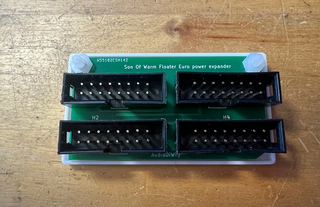
As my first FreeCAD project I created a tray for the Improved Warm Floater (initial post here)--the Warm Floater is a small PCB allowing 3 Euro modules to be powered by a single 16 conductor ribbon.  

The improved floater circuit board employs box headers in an effort to make it nearly impossible to orient the power cables incorrectly.  

I needed to create a tray for the PCB, insuring its contacts can't short against a conductive surface.

How did it go? So-so. Freecad is a complex program with a complex user interface; you won't be able to use it without a fair amount of study and practice.  

After a few evenings I got it working--fortunately there are almost endless youtube tutorial videos about FreeCad, although FreeCad's UI has changed over the years, so I had to refer to newer tutorials.

And I needed to remember: FreeCAD is free. No whining!

FREECAD WORKFLOW

I downloaded FreeCAD for Windows (here) and opened the program.
 
The first concept I had to understand was a FreeCAD "workbench". In FreeCAD parlance, your workbench is akin to a box of tools for building things.

For designing 3D parts like what's in today's post the workbench of choice was Part Design, chosen from a drop down in the main menu.

If I didn't choose the Part Design workbench, the steps below, their icons, their dialogs, and so on, didn't behave as expected or weren't visible at all.


In Part Design I create(d) a body then create(d) a sketch" (links were on the left side of the screen).  

I clicked on the XY-plane to anchor my sketch to it.  

Clicking OK, the workspace dropdown automatically changed to "Sketcher":


Sketcher is a 2D drawing tool, FreeCAD revolves around the idea of creating 2D drawing then turning them in 3D models. 

Using the 2D tools, I was ready to draw something in 2D; I created the outer rectangle of my tray.

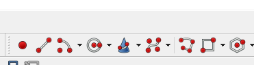
I found FreeCAD's icons to be confusing. For instance, here are 2D sketch tools. The rectangle and circle are obvious; The dunce cap? I still have no idea what the hell that one does.

Once I had my rectangle, I had to constrain it. I was unfamiliar with "constraining" my sketches, this meant, locking down the 2D proportions

A good video about how sketch constraints work is here.  A good design left no unconstrained dimensions; but at first I kept getting at least one "DOF" ("degree of freedom"--as in the online dating world, DOF is not always wanted) and found I was "under constrained" which in terms of coffee dates: about right.

Dof!!  
 

Constraining the shapes for my simple tray was easy enough however and after some practice constraining simple 2D shapes became pretty quick.  Update 7-12-25 for version 1.01 of Freecad you get at the basic constraint tools with an icon I hadn't seen before:


Clicking the down arrow you can see tools to constrain vertically, horizontally, set the radius or diameter of a circle and so on.

Once constraints were set, I clicked on CLOSE which closed the sketch and brought me back to the "part design" workbench.  A handy sketch tools dialog appeared, with choices like pad (which meant, extrude); hole (which allowed for tapered screwholes) and so on, but if I clicked anywhere else in FreeCAD this dialog went away and didn't readily come back....


....fortunately the same actions were found as icons along the top menu:


The next thing I did to my 2D shape was pad it (extrude it upward in the positive Z access).  OK, I padded to 3mm.

Next things got tricky. 

To create the tray I had to create a second sketch inside the first sketch, then"pocket" my design, "Pocket" is another FreeCAD term that was new to me.

This wasn't how I assumed you'd do this, why not have a command "make a lip" or whatever, but, nope. Every shape/cut/extrusion/screw hole in FreeCAD needed its own 2D sketch.  

I thought I could create this inner sketch by clicking the sketch icon in the main menu and creating another rectangle--but--nope. 

The 2nd sketch appeared to be hidden by the first. Drat!

I couldn't see this second sketch until I viewed the part from the bottom....that's where sketch 2 was created, BELOW the original one (not what I would have expected, nor what I wanted).  

What I need to do instead was choose the topmost plane of the initially created sketch by single clicking it.  

This "surface selection" (my term) only worked for creating additional sketches when the plane was the only thing colored:

Very important to make sure the surface I wanted my new sketch to sit on was colored, as you see here.  Otherwise the new 2D sketch didn't appear in a useful manner.

Now if I created a new sketch its Z origin sat on the green plane. Ah, that's what I wanted!

I created the inner sketch then constrained it to be exactly 1mm inside the first (is there another command "make the new sketch 1mm in every direction smaller than the one I just drew"? There must be....)

Finally clicked on a line of the inner sketch and clicked on the "pocket" icon. I chose a "dimension" pocket which was the default.

I entered 1mm and it worked.

Next, I needed 2 holes in the bottom of the tray.

When I tried adding the 2 holes to my first sketch I discovered once again--everything in FreeCAD with different Z extrusions had to be its own sketch and must sit on the correct plane.

I created a 3rd sketch, again choosing the surface I wanted the new sketches to sit on.  

This third sketch consisted of two constrained 3mm circles that would form the holes used to mount the PCB to the tray using nylon screws and nuts. 

Following the process above I "pocketed" the circles to push them though the inner tray (Sketch 2). 

I found no other way to do this, and this seemed like a whole lot of steps, that had to be done in exactly the right order, to make what I felt was an extremely simple 3D shape.  

But, it was done.

VIEWING THINGS IN FREECAD

To view or hide planes, you have to select the plane, right click, and say "toggle visibility". See the video here.

To zoom in or out use the mouse wheel.  Arrow keys move the imagine L/R or Up/Down.

To move around in 3D, hold the Shift key down along with the right mouse button. Click on an element in your part.  Now move the mouse. You knew this right? 

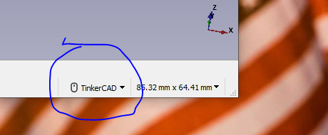
Probably not. Fortunately, I could change to different settings for rotating in 3D with my mouse (good video for setting up FreeCAD is here)--the "TinkerCad" choice is in the bottom right of the screen. Tinkercad allows 3D rotation using just the right mouse button. Better!


One more tidbit, you use "draft" workbench to create text. See the video here.

EXPORTING 3D MODELS TO KICAD

You need to install a 3rd party tool for this: KiCad StepUp.  Video on how to do this is here.  

The name of the tool is "Kicad StepUp. Once this tool is installed, I selected the body of my model and chose the KiCadStepUp workbench.  It threw an error "Requests not found" but I ignored that.

Then I clicked on the KSU export to Kicad button and used all the defaults. It told me where it saved my exported files (".wrl" and ".step" files) which I renamed and moved.  

The 3D image could now be imported into Kicad. I opened Kicad, and using Kicad's Footprint editor used the file > footprint properties > 3D model tab.
 

Update: FreeCAD allows exporting to WRL without a 3rd party tool. Select the entire 3D model; file > export. In Kicad: footprint editor; open a footprint; file > footprint properties > 3D tab.

TURNING THE DESIGN INTO TRAYS

With my tray finally done I printed one of these out on my 3D printer--which worked!--but needed more of them.  


So....With my tray STL file in hand, I whipped up a simple PCB uploaded both to PCBWAY, yes they do 3D printing, and wham, it was back. The 3D print jobs looked great. I am not saying this just because they're my sponsor, really, the quality of the print was top notch. 


Let's build!


3mm nylon screws and nuts fastens the PCB to the tray


This got mounted in my bench rack, now I can put more modules with low current draw in there....much needed improvement.

I figure I will get better at Freecad over time....this still feels very new to me. 

See ya next time. 


Warm Floater--Eurorack "Power Strip"

 Readers: If you want to build the power expander featured in this post, please go to PCBWAY's Community pages--a gerber ready to download and/or fabricate as well as KiCAD files, 3MF for 3D printing, FreeCAD files, etc. are here

Also please visit PCBWAY's site using the link here--it will help this blog. Thanks.

======

I solved a simple problem--I had too many Euromodules for my TipTop Happy Ending power supply. 

I didn't need more current, instead, I was out of physical connections.  

I whipped up a "power strip" for Eurorack--one 16 conductor input, 3 outputs. Small and simple....a one afternoon tops DiWHY project.


I laid it out in KICAD:

Using PCBWAY's Kicad Plug-In it's off to the blog's helpful sponsor--boom, it was back:


Building it was a piece of cake.


To test I hooked up three modules "op amp only" modules and checked the current draw--20mA. Fine.


Let's wire it up.


But! what happened if the traces shorted out against the case?  Electrician's tape!

At least I used green electrical tape!

But then I started to feel--guilty. Why not 3D print?  

Fusion360's license (for me) is going up from $100 a year to $795 a year--nope.

I started to check out an interesting--albeit counterintuitive and surprisingly hard to learn--CAD program called "FreeCad"--as a simple first project.  

FreeCAD and my brain were possibly not meant for each other. Nevertheless I designed a 3D WF Holder ("tray"? "backing"?) and printed it on my MP printer. You can download the 3MF file here and/or get it fabricated at PCBWAY, they do 3D printing all day long.

I had to widen the screw holes a bit to accommodate 5mm screws.  The 2 holes seen at the top of the PCB were enlarged in the uploaded gerber.

DONE! This is when it's good to know some DiWHY as I was seriously out of power plugs in my rack. This was a simple utilitarian PCB that I have not seem in the wild yet--it's probably out there and I missed it, if so, well now there are a few more of the damn things.

Again, you can download all the stuff for your own warm floater here.  

Next time, some MIDI.  See ya.

KicADSR: First Project Using KICAD EDA

 Readers: If you want to build the module featured in this post, please go to PCBWAY's Community pages--gerbers ready to download and/or fabricate as well as KiCAD files, PDF's, BOM etc., are here

Also please visit PCBWAY's site using the link here--it will help this blog. Thanks.

===================

Back again....from the previous post I switched from Eagle to Kicad for schematic capture and gerber file creation.  

To put KiCAD EDA to the test I laid out and fabricated a Eurorack synthesizer module I know pretty well: Rene Schmidt's "Fastest ADSR in the West".

Good news, the KiCAD based design, in Euro format, was easy to lay out, easy to troubleshoot and rework, and overall, works great. Success!


Posts about the last time I built the ReneDSR (in PAIA's Frac format) are here and here.

I originally laid this post's project with a lot of through hole resistors and whatnot, a 3 board design, but the highly skilled Elton from Otter Mods challenged me to use more SMD. So you will see a lot of 1206 SMD parts in this build as well.

Build photo time:

Happiness is new PCB's from this blog's patient sponsor, PCBWAY.

Two boards: main and front panel. Main board combines hardware and mostly SMD parts to allow the "skiff ready" 6HP footprint.


Testing as I go--the ICs are drawing correct amounts of current and not heating up.

Testing....

Oh Calcutta! Seems working.


SMD ADVANTAGES

Being afraid of my own shadow I set my bench up for SMD but continued to use through hole for most projects. 

KiCADSR uses through hole (or "THT" as Kicad calls it) components here and there, for instance, the 555 timer IC. 

Why? I didn't have SMD 555's in my junk box. 

Otherwise, for this new KiCAD era it was time to stop being wimpy about THT. 

Here's the thinking:

I don't need a microscope for everything SMD. I have bad eyesight but could work with 1206 sized parts, for the most part, wearing only reading glasses. 

SMD Parts turned out to be easier to swap after initial fabrication. Really? Yes. I soldered a 220ohm resistor between the voltage rails instead of 100K. Needless to say this was not a good idea and the part heated up quickly. 

Replacing a THT resistor in this kinda situation wouldn't have been impossible but may not have been easy either. I could have lifted a trace for instance. With SMD it was easy! I heated up the part's pads quickly with my iron--each in succession--then lifted it out with tweezers; cleaned up the pads with wick and soldered the new part. I also experimented using my rework tool for this. No, all the parts on the board didn't melt off. No, I didn't make a huge mess. I found both processes quicker and easier than using a solder sucker to remove THT parts.

I didn't need as much room to store parts. I have a whole wall of bins for THT parts, but only a few small boxes for SMD. At some point SMD makes more sense in this regard as my psychiatrist wife (no longer my psychiatrist girlfriend--update, we got married, she is so wonderful, and I got very, very lucky) can't give up endless domestic space to my puzzling hobby.

I could put annoying .1uF filter caps on the back side of the PCB to save space.  In fact, I could have distributed parts on both sides, not just filter caps. 

For the KiCADSR I put one .1uF cap on the board's backside, then wondered why I didn't put all the filter caps on the back side. So if you build this, make sure to flip the main PCB and solder on that part.

In general I found I could fit a lot more circuitry in a smaller space with SMD, and too damn much of Eurorack is all about everything being really tiny.

Redoing incorrect traces is easier when using SMD.  This one was hard to believe. I had 3 fixes necessary to get KiCADSR to work:  I missed a trace during schematic capture and 2 of the pins on the 3.5mm jacks were swapped. Quickly fixed. To wit:

FIXES

Three--count 'em--THREE fixes were needed.  To my surprise: not too hard to solder these fixes in with SMD

Elton was right, kludging fixes with SMD was easier than I thought: I prepped and tinned some 22 gauge wire and soldered it to the butts of the appropriate components. I thought this was going to suck but at the end of the day was it easy. Note: the project I posted at PCBWAY community (here) already has the fixes and the symbol library at github (here) has the updated parts. I have tested this updated PCB working.

OUTTRO

KiCAD is vastly superior to Eagle, and SMD is superior in many ways to THT. It's taken me years of being told this to finally take it to heart, but maybe now I have.

Too often I am too set in my ways to move on--until I actually move on--and only then realize I should have moved on a long time ago. Is there a lesson in here somewhere?  Yes, but I will almost certainly continue to ignore it.


Kicad: Making the Switch

Bad news (for me). 

Autodesk's Eagle is the schematic capture/PCB layout application--"Electronics Design Automation" or "EDA"--I've been using forever.  

But starting in 2026 Autodesk wants $749 USD a year for a Fusion 360 integrated version--and I confirmed with their sales team: my existing $100/year Eagle/Fusion 360 license is going away.

Time to say goodbye to Eagle. 

Say Hello to KiCad.


The guys in my geeky synth meetup group have been telling me to use Kicad for years. Now, everyone will be be happy?  

This post captures notes written during my initial exposure to KiCAD 7. 

As usual this blog post is my own trail of breadcrumbs. If you are thinking of switching to Kicad from another EDA, or are a Kicad newbie like me, the post may be of some use. 

Otherwise, you may want to skip this one.

GET KICAD

$749? Nope. KiCAD is free. Download it here.  

I got the Windows version--not sure how transparent going between OS's will be, cross platform compatibility was poorly implemented in Eagle. Kicad docs say it's transparent; no reason to doubt them. I will try opening PC created projects on Linux and Mac down the road. I had no problem installing it on a few Windows 10 systems.

PROJECTS

Eagle and Kicad allow me to create a "project"; I never used projects in Eagle. Instead, I created a folder using my OS and put Eagle schematics and boards in there--as many schematics and PCB files in a single folder as I wanted; it was easy to have many schematic revisions in a single folder as long as each had a unique filename and the correct file extension....it all worked.

KiCAD is different; it is designed around a single project/single schematic/single board paradigm. However, a single schematic can have "subsheets" (details here--I have not tried subsheets yet).

Creating a new Kicad project creates new helper files and folders, so if I want to create a revised PCB for a given project, or create an additional board (a "revision 2.0" for example) I have to:

  • Use Windows Explorer to create a new folder
  • Copy the original project (.pro), schematic (.sch), and PCB (.pcb) files into the new folder 
  • Rename the project, PCB, and schematic files to a matching filename (with their original .kicad* extensions intact) 
Automating these steps should be easy using something like Python and Powershell. I will look around for a script or macro for this. I'd be surprised if someone hasn't already created a utility for spinning off versions of Kicad projects, but so far I can't find it. Update 5-15-25: Kicad V9 has a "save as" under "file"....which creates a duplicate of the current project. You can see the save as menu item when you open a Kicad project, before you open your schematic or PCB. 

KICAD LIBRARIES: SYMBOLS AND FOOTPRINTS 

Eagle has a devilishly confusing "device/symbol/footprint" paradigm that makes you pick a symbol and footprint while choosing a component for your schematic. Eagle "device libraries" contain all the necessary elements--the symbol, the footprint, and how the two interconnect.

After using Eagle EDA for over 20 years I still find creating and managing custom or modified devices confusing, frustrating, and teeth-gnashingly counterintuitive.

KiCAD is a HUGE improvement--symbols and footprints have their own libraries and each is managed separately. The user has to make sure pins and pads are laid out correctly, but that's the case in Eagle as well. 

For a good primer on Kicad symbol creation the video here; footprint creation here. The same ideas are used to modify existing objects as creating new ones. It's easy!

Elton from OtterMods, the resident KiCAD expert in my synth MeetUp group, suggested creating a custom personal library composed of symbols and footprints to be used over and over. Some are made "from scratch", some are brought in from snapEDA, some from obscure libraries found on the Internet, some are existing KiCAD library objects with minor modifications.

Following Elton's lead, I created, and will maintain, custom Kicad symbol and footprint repos. I have posted that on GitHub; go here and here.

Update 3-2-25: All hail smisioto.no--you can find most every Kicad symbol/footprint/3d model you could ever think of, and a lot you never thought of: here. Wow!

SCHEMATIC CAPTURE

After only using Kicad for a few hours, I found its schematic capture ability (well documented here) to be really easy!  

A few shortcuts proved helpful:

  • A for adding new symbols; basics like resistors and capacitors are in the folder called "devices".  Shortcut: type "C" for a generic cap symbol and "R" for a generic resistor symbol.
  • M for move 
  • D for drag.  This is the same as "moving" in Eagle--you can move a part and the wires won't break.
  • R, X or Y for rotating and mirroring
  • W for wiring; / (slash) changes if you want to allow 90 degree bends in your wiring, 45 degrees, etc.
  • E for modifying a symbol's properties....tap this and a dialog pops up when you can change things like values, display characteristics, fonts, and whatnot--this "E" behavior seems universal to many objects in Kicad. You also see options for changing symbols for your entire schematic through the "E" shortcut.

Right click > change symbol brings up a dialog to replace one symbol with another. This is the same as right click > replace in Eagle.

Synchronizing modified or updated "devices" in Eagle into my design was always cumbersome and confusing. Thank goodness it's much easier in Kicad--edit a custom symbol using the "symbol editor", save, open the schematic, then issue Tools -->update symbols from library. This brings up a dialog where you can find and replace symbols found in the entire schematic or a subset. This synch process has to be done manually; fine with me.

Tools > assign footprints brings up the dialog where you can assign footprints for your symbols. Again I found this pretty straightforward with one space oddity: to make your choices "stick" you have to click the "Apply, Save Schematic and Continue" button after making your edits--just clicking OK won't do it.


Another Kicad feature: You can modify a PCB and have the changes brought back into the schematic.  Tools > update schematic from PCB. Eagle can't do this.

There are a lot more options and features of course. Thankfully Kicad's documentation is really good--find it here.  

Update: I see this schematic layout elements of Kicad called "EESCHEMA".  I am not an EE, but I occasionally have a SCHEMA.

LAYING OUT PCB's

Eagle automatically creates a PCB from your schematic; with Kicad, you have to start up the PCB editor then issue the command tools > update schematic from PCB to see footprints.

The PCB creation documentation (here) has a lot of detail, but I found the basics to be pretty easy once I learned some shortcuts:

  • D  drag a part, moving its traces along with it. If a trace turns green during the attempt it means it conflicts with your relocated footprint--edit conflicting trace(s) and try again. Otherwise--if you don't remember to hit D--the footprint will move but not its traces and you are left with a mess. Is there a way to make D the default behavior?
  • X turns on the "trace route" tool
  • Page up/page down toggles between layers (front and rear copper for instance)
  • V places a via
  • For 2 layer boards, the quick way to switch between placing front and back traces: create your trace, click "V" on your keyboard, placing a via, and then left click with your mouse to continue running a trace on the opposite side of your PCB. Don't click any other keys (no shift, no control, no enter) or this workflow may be interrupted.   
  • Alt + 3 shows a 3D view of the PCB (cool!!!)
  • There are many more shortcuts documented here.

right click -- drag from bottom to top selects everything; right click -- drag top to bottom selects only items fully enclosed. Useful! Video here.

To change trace width, it's easy with Eagle--type in "change width 10 mil" or whatever in the uppermost text box then click on a trace that you want to fatten.

A few more steps with Kicad, but still not hard:

In the PCB editor, choose Track: use netclass width > edit predefined sizes.


Next, hit the + below then add some sizes to the dialog. (By the way: 40mm-75mm are really big trace sizes--I was messing around with DRC--you probably want smaller traces...)


Hit OK, now you can dial in the track width you want from the same "Track: use netclass width" when creating traces.


IMPORTING FROM EAGLE

Update: 3-3-25 I have removed this section re: the Eagle > Kicad update process for Kicad 7 since it's changed and is much improved in Kicad 8 and 9.

If interested, please read the dedicated post--Kicad >= 8 imports from Eagle--here.

BLOCKS AND HIERARCHICAL SHEETS

Modularity and reuse in Kicad? You bet! I removed that from this post because after many edits the section was getting too long; dedicated post on these features is here.

"LIVE AND LEARN"

....solutions to things I had to figure out, not immediately obvious to me

Changing footprint descriptions; matching a footprint to its 3D image Surprisingly--neither are available via the "e" shortcut. With the footprint open and ready to edit: file > footprint properties. The "General" tab allows you to change the description; "3D Models" lets you select then position 3D images for the footprint. 11-20-23

Changing "drawing sheet" size (the border with title block etc): open EESCHEMA editor or PCB editor, then > file > page settings.  Adjust width and height. 11-25-23 
 
Creating ground pours: I always forget how to do this...we will start with the front layer:
  • open your PCB 
  • In the top right, under "Appearance", left click on "F. Cu":


  • to the right of your PCB, click on this icon:


  • Left click somewhere outside your PCB's edgecut
  • Select "F.Cu" and "GND" (or whatever designation you are using for ground) in the dialog that appears:


  • Draw a rectangle around your entire PCB, doesn't matter where, but make it bigger than your edge cuts
  • Hint: when closing your rectangle right click + "close outline" to complete the rectangle
  • Click B on your keyboard to fill.
  • Run Inspect > Design Rules Checker to make sure the pour is OK.
Repeat the process for the B.cu (bottom layer). 

Cool, but how to turn the damn pours off when you want to edit your PCB?
The "toggle your pours on and off" icons are on the left side of the PCB:


 Good video for this is here2-9-24

Making imported footprints work with Kicad symbols: This is an obvious one that I missed for several weeks.

Eagle allows you to name device pins--"Tip", "Ground", and "Sleeve" for a 3.5mm jack, for instance. I figure all EDA programs do this.

But! Corresponding Kicad pins have numbers, not names; pin numbers in Kicad may not match those imported from Eagle,

When importing Eagle devices into Kicad custom libraries: edit pin numbers to make them Kicad-like. 

"Kicad-like?" 

Here is what I mean: Kicad symbols often follow a pattern: for instance, for diodes, it's usually 2-anode and 1-cathode. So if you are importing an Eagle diode into a custom Kicad library, edit your imported footprint to change pin names "Anode" to "2" and "cathode" to "1".

If there is any doubt open a factory symbol in Kicad and note its pin numbers. Then, edit the Eagle component before adding to your custom libraries so it will work in future designs. 5-26-24
 
Constraining lines to H/V/45 degrees: when drawing silkscreen lines for boards for instance, right click as you are drawing and choose "H/V/45".  This constrains the line to Horizontal, Vertical, and 45 degrees. Nice! To undo, right click again as you are drawing and deselect this feature. 5-31-24

Placement Constraint: This assumes Preferences > Preferences >  Schematic Editor (or) Footprint Editor > Grid Display >Snap to Grid is set to "Always" or "when grid is shown":


Use the UI element boxed in red below to constrain line endpoints, parts placements, text locations, etc. 

This setting does not impact the density and frequency of visible cross hatches/dots/lines as you zoom in and out; instead, it determines where by default you can place things.  


Holding down "control" while placing an object overrides this setting.  9-1-24

Importing 3D models into Kicad: Save your 3D file in "STEP", "STP". or ".WRL" format--most 3D software can do this. Then: open the footprint editor in Kicad, choose the footprint that needs a 3D model, then file > footprint preferences > 3D tab. Click the folder icon at the top of the dialog and choose your WRL or STP file you just saved; use the various +/- buttons to scale and position your model. When you're happy, click OK. Good video for this can be found here9-14-24

Importing .lib symbol libraries into Kicad: seems <= Kicad 5.0 (?) used ".lib" as an acceptable extension for a symbol library. If you are importing from the outside world (e.g. the useful library here) you might find 2 files: .dcm and .lib.  Leave .dcm alone but rename the extension of the .lib file to .kicad_sym; open symbol editor in Kicad  > import the library > find the .kicad_sym file > OK  9-30-24

Importing symbols into Kicad: You can't overwrite the symbol libraries that shipped with Kicad, so you'll need to save imported symbols into their own symbol library then import it into your project (how-to here). 

Better yet, extract the symbols you care about into your own custom symbol (*.kicad_sym) file. 

How to do the latter.

Create a custom library if you don't already have one (symbol editor > file > new library), or get my custom symbol library from Github here, save it to your hard drive, then add your cool symbols to it.

To import a single symbol into your custom symbol library: 
  • Save your newly acquired .kicad_sym file somewhere.
  • Unzip the symbol file if needed
  • In KiCad, go to Preferences.
  • Click on Manage Symbol Libraries.
  • On the Global Libraries tab, click on Browse Libraries (the small folder icon)
  • Select the .kicad_sym file you just imported, then click Open.
  • The library will appear, click OK.
  • From the main Kicad screen, click on Symbol Editor.
  • Type on the filter search field and navigate to the symbol in the library you just imported.
  • Double-click it to open the file.
  • Edit the symbol as needed 
  • Optional: File > symbol properties > footprint and assign the symbol a default footprint
  • File > save copy as  
  • Save the symbol, extracted from the imported library, into your custom symbol library.   10-28-24
Kicad Symdirs:  In kicad10, you can create a folder called [foldername].kicad_symdir and save your custom symbols there. This makes editing them the same mindset as editing as footprints: edit a single custom symbol and not have to resave the entire symbol library, rather, just your newly modified symbol. Nice! Get my custom symdir content from github here5-21-26

Setting Grid Origins for your PCB:  (tried this with Kicad V9, not sure about older versions) By default 0,0 of my grid is the top left corner the large purple box that holds your PCB drawing--the "drawing sheet"?  Sorry still don't know what to call the purple box thing. 

I don't want 0,0 to be there since it has nothing to do with my PCB. I want it to be the bottom left corner of my PCB. How to change this?

  • In the PCB editing tool, set your grid--say 100 mils--from the pull down at the top:


  • Select then move your entire PCB so the bottom left corner of the edge cut lines up with a sensible spot on the grid.
  • Preferences > Preferences > PCB Editor > Origins & Axis 
  • Choose "Grid Origin":
  • Go back to your PCB, and from the menu along the top: Place > Grid origin
  • left click on bottom left corner of edge cut. You will see a cross on the new origin.  5-17-25
Getting started with NGSpice Simulations and Kicad: Complex enough that it needs its own post; go here. 2-10-25

Why can't I select a @#$% symbol library to import things into?  Simple! make sure this icon is selected on one of the left columns. Your list of available symbol libraries appears...left-click on to select a symbol library to import things into. Remember! you can't import anything nor edit the "stock" libraries that come with Kicad--you have to use a 3rd party library or create your own. 4-25-26 (Kicad 10)


Avoid using absolute paths for things like custom 3D models. Use "Environment Variables" instead. 

A path like this maps to a windows D:\ drive and will work on a single system:


But as soon as you go to any system that has "Dropbox" mapped to somewhere else on its local storage devices this will break.  

Instead, use a Kicad Environment variable:


Notice the syntax here: ${env_variable_name}

You can create as many custom variables as you want, configure this through Preferences > Configure paths:


You can then drop these variables into things like "where does the 3D file for this live"?  This will allow a computer with different directory locations to still find things you create in Kicad.

  4-26-26 


OUTRO: GERBERS n' PCBWAY 

In case you haven't noticed by now, Kicad kicks Eagle's butt. Small wonder Autodesk is moving on.

After a few evenings with Kicad, I feel I know enough to create a baptism-by-fire schematic and PCB. Probably a retread of something I made in Eagle? Why not....coming soon.  

HA!!--it works--"KicADSR".  My first Euro module created with Kicad. Post is here.

Not that kinda gerber....

....I checked out a Kicad gerber creation how-to on my sponsor PCBWAY's site--here.  

Check that! Shout out to Serene at PCBWAY, she told me I could get PCBWAY's add-on for Kicad--for uploading designs to PCBWAY for fabrication using a single click. 

Instructions for setting up the plug-in are here.  

A useful video going over other cool Kicad add-ons is here.

After installation the plug-in made uploading files to PCBWAY a breeze: I logged into the PCBWAY website, ran Kicad, opened the test PCB, the in Kicad went to tools > plug-in > "PCBWAY Plug-in for Kicad".   

This gerber-ized my file and everything looked to be good to go.

Finally I picked which color PCB I wanted, how many I wanted fabricated, any a few other options; then hit "add to cart".....

Enough for now, this is getting to be long post. Much more KiCAD on the way. Don't breathe the fumes....  


ARP 2600 Voltage Processor The Final Chapter: ARP Electronic Switch: the Workalike Works

 Readers: If you want to build the module featured in this post, please go to PCBWAY's Community pages--a gerber ready to download and fabricate is here

Also please visit PCBWAY's site using the link here--it will help this blog. Thanks.

===========

Hello again! Finishing up ARP 2600 voltage processor clones and workalike modules, this might be the last of the series, which is not a bad thing?  

The ARP2600's unique voltage processor has a click- and pop-free clock-driven analog electronic switch for AC and DC signals. 

You can find the original design on page 29 of the ARP 2600 service manual here.

The 70's era subcircuit used discrete components for its toggle flip-flop and employed LS4392 FETS for heavy lifting.

Best of all: a working Electronic switch completes my ARP2600 voltage processor series. Are we home yet?

Finished ARP2600 Electronic Switch workalike

I decided to use a DG401 IC instead of the FETS--post where I initially experimented with that IC is here with more here.

In short: The DG401 works great--think of a rail to rail version of the venerable 4051 analog CMOS switch; both are useful chips for a lot of what we do.

I laid out PCB's for the workalike and sent them to the blog's patient sponsor, PCBWAY, to create a 5HP Euro prototype.

Let's see if what I designed works....

Happiness is new PCB's from PCBWAY....

The build uses about 2/3rd's SMD components, many of which I don't have in the junk box. I bought the parts from Digikey and posted the BOM on the PCBWAY community page (here).

Unpopulated main board--I am getting more comfortable with1206 SMD components--large enough that I don't need a microscope for a lot of the work. 


Front panel....


Testing....


Did it "work first time"?  

Kinda. 

The switch switched somewhat randomly unless I used a square or pulse wave. During the breadboard stage, triangles and some ramps switched same as a square wave, but in this layout, not as much.

Not sure why....on the bench (breadboarded) here's what I used to buffer the incoming clock signal:

But for this post's Euro module triangle and ramp incoming signals created switching "warbles". 

Not intended, but not a bad thing?  I could have spent days chasing this down--for instance, setting up the breadboard and expermenter's board for the DG401 and double checking my work--redesigned the buffer using an MCU to turn whatever input to a pulse wave--using an op amp with a diode in its negative feedback path--something has to work, right? 

But, naaaaaah. 

Too many other things to do.  

Instead I replaced the .1µF cap with a 1K resistor. That's surprising quick and easy with 1206 SMD parts: heat up both sides of the .1µF capacitor with a soldering iron in quick succession; use tweezers to remove the cap, then solder in a 1206 1K SMD resistor.  

Done.

With that modification square and pulse waves work great to make the DG401 switch.  

Good enough....the workalike switches cleanly, no delays, no clicks, no pops, same to my ears as the ARP2600.   

And! The "any waveform to clock" apparently isn't implemented on the original gazillion dollar collectable 2600 my friend owns....so I could argue that the design flaw makes this workalike more akin to the original.

Not a feature--a bug. 

Time to move on!  

Next time--no idea. How about this: I'm ditching Eagle for Kicad since Autodesk is raising my annual subscription price 700 percent. So I may do a few less posts in the next few weeks while I learn this new program. Go A's